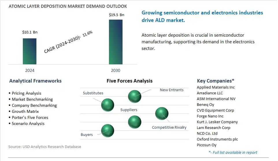
The global Atomic Layer Deposition Market is poised to register a 11.6% CAGR from $10.1 Billion in 2024 to $19.5 Billion in 2030.
The global Atomic Layer Deposition Market Study analyzes and forecasts the market size across 6 regions and 24 countries for diverse segments -By Product (Thermal ALD, Metal ALD, Plasma-Enhanced ALD, Others), By Application (Electronics & Semiconductors, Solar Devices, Medical, Others).
An Introduction to Global Atomic Layer Deposition Market in 2024
The atomic layer deposition (ALD) market is witnessing rapid growth driven by increasing demand in semiconductor manufacturing, electronics, and energy storage applications for thin film deposition and surface engineering. Key trends shaping the future of the industry include the growing adoption of ALD for precise and conformal film deposition on complex substrates, enabling advanced device architectures, miniaturization, and performance enhancement. Moreover, there's a rising emphasis on ALD-enabled materials innovation for emerging technologies such as nanoelectronics, photovoltaics, and biomedical devices, leading to collaborations between ALD equipment suppliers, materials developers, and research institutions. Additionally, advancements in ALD process control, reactor design, and precursor chemistry are driving innovation and market expansion, enabling ALD manufacturers to offer scalable and cost-effective solutions for high-volume production and technology development in the global atomic layer deposition market.
Atomic Layer Deposition Market Competitive Landscape
The market report analyses the leading companies in the industry including Applied Materials Inc, Arradiance LLC, ASM International NV, Beneq Oy, CVD Equipment Corp, Forge Nano Inc, Kurt J. Lesker Company, Lam Research Corp, NCD Co. Ltd, Oxford Instruments plc, Picosun Oy, SENTECH Instruments GmbH, Veeco Instruments Inc.
Atomic Layer Deposition Market Dynamics
Atomic Layer Deposition Market Trend: Increasing Adoption in Nanotechnology and Semiconductor Industries
A prominent market trend for atomic layer deposition (ALD) is its increasing adoption in nanotechnology and semiconductor industries. ALD is a thin film deposition technique known for its precise and uniform layer-by-layer deposition process, making it ideal for fabricating nanoscale structures and semiconductor devices with high precision and control. As industries such as electronics, photonics, and nanotechnology continue to advance, there's a growing demand for ALD technology to enable the production of next-generation devices, including advanced transistors, memory devices, sensors, and optical coatings. This trend drives market growth for ALD equipment, materials, and services as manufacturers and researchers leverage ALD technology to develop innovative products and enhance device performance in various applications.
Atomic Layer Deposition Market Driver: Semiconductor Industry's Demand for Miniaturization and Performance Enhancement
A significant driver for the atomic layer deposition market is the semiconductor industry's demand for miniaturization and performance enhancement in electronic devices. With the ongoing trend of Moore's Law and the continuous shrinking of semiconductor feature sizes, there's a need for deposition techniques that can deposit ultra-thin films with precise thickness control and uniformity. ALD technology addresses this demand by offering sub-nanometer thickness control and excellent conformality, allowing manufacturers to deposit thin films on complex 3D structures and achieve high-density integration in semiconductor devices. As semiconductor manufacturers strive to enhance device performance, reduce power consumption, and overcome manufacturing challenges associated with scaling, the demand for ALD equipment and materials continues to grow, driving market expansion in the semiconductor industry.
Atomic Layer Deposition Market Opportunity: Expansion into Emerging Applications such as Energy Storage and Catalysts
An opportunity for the atomic layer deposition market lies in the expansion into emerging applications beyond the semiconductor industry, such as energy storage and catalysts. While ALD technology is well-established in semiconductor fabrication, its unique capabilities for precise film deposition and surface engineering make it suitable for a wide range of emerging applications in energy storage devices, such as lithium-ion batteries, fuel cells, and supercapacitors. Additionally, ALD is gaining traction in catalyst synthesis and surface modification for catalytic converters, hydrogen production, and environmental remediation applications. By exploring new application areas outside of the semiconductor industry, ALD equipment suppliers, materials manufacturers, and service providers can diversify their customer base, expand into new market segments, and unlock opportunities for growth and innovation in emerging technology fields.
Atomic Layer Deposition Market Share Analysis: Thermal ALD segment generated the highest revenue in the industry
Among the products in the Atomic Layer Deposition (ALD) Market, thermal ALD segment is the largest, and diverse factors contribute to this status. Thermal ALD is one of the most established and widely used techniques in the field of ALD, offering precise control over film thickness and composition with excellent uniformity and conformity. In thermal ALD, precursor molecules are alternately pulsed into a reaction chamber, where they react with the substrate surface to form a monolayer of thin film material. This process is carried out at relatively low temperatures, below 300°C, making it compatible with a wide range of substrates, including semiconductors, glass, and polymers. In addition, thermal ALD provides excellent film quality and stoichiometry control, making it suitable for various applications such as semiconductor device fabrication, catalysis, and surface modification. Additionally, the simplicity and scalability of thermal ALD systems make them attractive for both research and industrial applications, contributing to their widespread adoption in the market. While other ALD techniques such as metal ALD and plasma-enhanced ALD offer specific advantages for certain applications, thermal ALD remains the largest segment due to its versatility, reliability, and well-established track record in the ALD industry.
Atomic Layer Deposition Market Share Analysis: Electronics & Semiconductors Segment is poised to register the fastest growth rate (CAGR) over the forecast period to 2030
The Electronics & Semiconductors segment is the fastest-growing sector within the Atomic Layer Deposition (ALD) Market, driven by diverse key factors. ALD plays a crucial role in the fabrication of advanced electronic and semiconductor devices by enabling precise deposition of ultra-thin films with atomic-level control over thickness and composition. In the semiconductor industry, ALD is widely used for depositing high-k dielectric materials, metal gate electrodes, diffusion barriers, and passivation layers in advanced CMOS (Complementary Metal-Oxide-Semiconductor) devices. As semiconductor manufacturers continue to scale down device dimensions and transition to 3D architectures to meet the demands of Moore's Law, the importance of ALD in achieving precise film thickness control, excellent uniformity, and conformal coverage becomes increasingly critical. In addition, ALD offers unique advantages such as low-temperature processing, enabling the deposition of thin films on temperature-sensitive substrates and integration with existing semiconductor manufacturing processes. Additionally, the growing demand for advanced electronic devices, including smartphones, tablets, IoT (Internet of Things) devices, and automotive electronics, drives the adoption of ALD in the electronics industry. Further, emerging applications such as memory devices, MEMS (Micro-Electro-Mechanical Systems), and advanced packaging further expand the market opportunities for ALD in the electronics and semiconductor sectors. With continuous technological advancements and increasing demand for high-performance electronic devices, the Electronics & Semiconductors segment is expected to experience rapid growth in the ALD Market.
Atomic Layer Deposition Market Report Segmentation
By Product
Thermal ALD
Metal ALD
Plasma-Enhanced ALD
Others
By Application
Electronics & Semiconductors
Solar Devices
Medical
Others
Regions Included
North America (US, Canada, Mexico)
Europe (Germany, UK, France, Spain, Italy, Russia, Rest of Europe)
Asia Pacific (China, India, Japan, South Korea, Australia, South East Asia, Rest of Asia)
South America (Brazil, Argentina, Rest of South America)
Middle East and Africa (Saudi Arabia, UAE, Rest of Middle East, South Africa, Egypt, Rest of Africa)
Atomic Layer Deposition Companies Profiled in the Market Study
Applied Materials Inc
Arradiance LLC
ASM International NV
Beneq Oy
CVD Equipment Corp
Forge Nano Inc
Kurt J. Lesker Company
Lam Research Corp
NCD Co. Ltd
Oxford Instruments plc
Picosun Oy
SENTECH Instruments GmbH
Veeco Instruments Inc
*- List Not Exhaustive
TABLE OF CONTENTS
1 Introduction to 2024 Atomic Layer Deposition Market
1.1 Market Overview
1.2 Quick Facts
1.3 Scope/Objective of the Study
1.4 Market Definition
1.5 Countries and Regions Covered
1.6 Units, Currency, and Conversions
1.7 Industry Value Chain
2 Research Methodology
2.1 Market Size Estimation
2.2 Sources and Research Methodology
2.3 Data Triangulation
2.4 Assumptions and Limitations
3 Executive Summary
3.1 Global Atomic Layer Deposition Market Size Outlook, $ Million, 2021 to 2030
3.2 Atomic Layer Deposition Market Outlook by Type, $ Million, 2021 to 2030
3.3 Atomic Layer Deposition Market Outlook by Product, $ Million, 2021 to 2030
3.4 Atomic Layer Deposition Market Outlook by Application, $ Million, 2021 to 2030
3.5 Atomic Layer Deposition Market Outlook by Key Countries, $ Million, 2021 to 2030
4 Market Dynamics
4.1 Key Driving Forces of Atomic Layer Deposition Industry
4.2 Key Market Trends in Atomic Layer Deposition Industry
4.3 Potential Opportunities in Atomic Layer Deposition Industry
4.4 Key Challenges in Atomic Layer Deposition Industry
5 Market Factor Analysis
5.1 Value Chain Analysis
5.2 Competitive Landscape
5.2.1 Global Atomic Layer Deposition Market Share by Company (%), 2023
5.2.2 Product Offerings by Company
5.3 Porter’s Five Forces Analysis
5.4 Pricing Analysis and Outlook
6 Growth Outlook Across Scenarios
6.1 Growth Analysis-Case Scenario Definitions
6.2 Low Growth Scenario Forecasts
6.3 Reference Growth Scenario Forecasts
6.4 High Growth Scenario Forecasts
7 Global Atomic Layer Deposition Market Outlook by Segments
7.1 Atomic Layer Deposition Market Outlook by Segments, $ Million, 2021- 2030
By Product
Thermal ALD
Metal ALD
Plasma-Enhanced ALD
Others
By Application
Electronics & Semiconductors
Solar Devices
Medical
Others
8 North America Atomic Layer Deposition Market Analysis and Outlook To 2030
8.1 Introduction to North America Atomic Layer Deposition Markets in 2024
8.2 North America Atomic Layer Deposition Market Size Outlook by Country, 2021-2030
8.2.1 United States
8.2.2 Canada
8.2.3 Mexico
8.3 North America Atomic Layer Deposition Market size Outlook by Segments, 2021-2030
By Product
Thermal ALD
Metal ALD
Plasma-Enhanced ALD
Others
By Application
Electronics & Semiconductors
Solar Devices
Medical
Others
9 Europe Atomic Layer Deposition Market Analysis and Outlook To 2030
9.1 Introduction to Europe Atomic Layer Deposition Markets in 2024
9.2 Europe Atomic Layer Deposition Market Size Outlook by Country, 2021-2030
9.2.1 Germany
9.2.2 France
9.2.3 Spain
9.2.4 United Kingdom
9.2.4 Italy
9.2.5 Russia
9.2.6 Norway
9.2.7 Rest of Europe
9.3 Europe Atomic Layer Deposition Market Size Outlook by Segments, 2021-2030
By Product
Thermal ALD
Metal ALD
Plasma-Enhanced ALD
Others
By Application
Electronics & Semiconductors
Solar Devices
Medical
Others
10 Asia Pacific Atomic Layer Deposition Market Analysis and Outlook To 2030
10.1 Introduction to Asia Pacific Atomic Layer Deposition Markets in 2024
10.2 Asia Pacific Atomic Layer Deposition Market Size Outlook by Country, 2021-2030
10.2.1 China
10.2.2 India
10.2.3 Japan
10.2.4 South Korea
10.2.5 Indonesia
10.2.6 Malaysia
10.2.7 Australia
10.2.8 Rest of Asia Pacific
10.3 Asia Pacific Atomic Layer Deposition Market size Outlook by Segments, 2021-2030
By Product
Thermal ALD
Metal ALD
Plasma-Enhanced ALD
Others
By Application
Electronics & Semiconductors
Solar Devices
Medical
Others
11 South America Atomic Layer Deposition Market Analysis and Outlook To 2030
11.1 Introduction to South America Atomic Layer Deposition Markets in 2024
11.2 South America Atomic Layer Deposition Market Size Outlook by Country, 2021-2030
11.2.1 Brazil
11.2.2 Argentina
11.2.3 Rest of South America
11.3 South America Atomic Layer Deposition Market size Outlook by Segments, 2021-2030
By Product
Thermal ALD
Metal ALD
Plasma-Enhanced ALD
Others
By Application
Electronics & Semiconductors
Solar Devices
Medical
Others
12 Middle East and Africa Atomic Layer Deposition Market Analysis and Outlook To 2030
12.1 Introduction to Middle East and Africa Atomic Layer Deposition Markets in 2024
12.2 Middle East and Africa Atomic Layer Deposition Market Size Outlook by Country, 2021-2030
12.2.1 Saudi Arabia
12.2.2 UAE
12.2.3 Oman
12.2.4 Rest of Middle East
12.2.5 Egypt
12.2.6 Nigeria
12.2.7 South Africa
12.2.8 Rest of Africa
12.3 Middle East and Africa Atomic Layer Deposition Market size Outlook by Segments, 2021-2030
By Product
Thermal ALD
Metal ALD
Plasma-Enhanced ALD
Others
By Application
Electronics & Semiconductors
Solar Devices
Medical
Others
13 Company Profiles
13.1 Company Snapshot
13.2 SWOT Profiles
13.3 Products and Services
13.4 Recent Developments
13.5 Financial Profile
Applied Materials Inc
Arradiance LLC
ASM International NV
Beneq Oy
CVD Equipment Corp
Forge Nano Inc
Kurt J. Lesker Company
Lam Research Corp
NCD Co. Ltd
Oxford Instruments plc
Picosun Oy
SENTECH Instruments GmbH
Veeco Instruments Inc
14 Appendix
14.1 Customization Offerings
14.2 Subscription Services
14.3 Related Reports
14.4 Publisher Expertise
By Product
Thermal ALD
Metal ALD
Plasma-Enhanced ALD
Others
By Application
Electronics & Semiconductors
Solar Devices
Medical
Others
Countries Analyzed
North America (US, Canada, Mexico)
Europe (Germany, UK, France, Spain, Italy, Russia, Rest of Europe)
Asia Pacific (China, India, Japan, South Korea, Australia, South East Asia, Rest of Asia)
South America (Brazil, Argentina, Rest of South America)
Middle East and Africa (Saudi Arabia, UAE, Rest of Middle East, South Africa, Egypt, Rest of Africa)