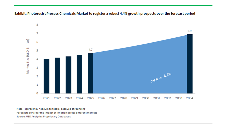
Photoresist Process Chemicals Market Size 2025–2034: $4.7 Billion to $6.9 Billion at 4.4% CAGR Powered by EUV Lithography Expansion and AI Semiconductor Scaling
The global photoresist process chemicals market is projected to grow from $4.7 billion in 2025 to $6.9 billion by 2034, registering a CAGR of 4.4%. This market encompasses high-purity photoresist developers, anti-reflective coatings (BARC/TARC), underlayers, edge bead removers, strippers, post-CMP cleaners, and specialized lithography ancillaries required for advanced semiconductor manufacturing. As logic and memory nodes move toward 2nm, 1.4nm, and sub-1nm architectures, the demand for ultra-clean, defect-minimizing process chemistries is intensifying. The commercialization of High-NA EUV lithography and advanced packaging technologies is structurally expanding consumption volumes of photoresist process chemicals across foundries and IDMs.
Japan reinforced its leadership in semiconductor lithography materials through strategic consolidation in 2024. On December 1, 2024, JSR Corporation formally merged with JICC-02 following a $6.4 billion acquisition by Japan Investment Corporation. This privatization enhances long-term investment flexibility for next-generation EUV photoresists and supporting process chemicals required for sub-1nm nodes. In parallel, Shin-Etsu Chemical is progressing toward 2026 completion of Phase 1 at its ¥83 billion Gunma manufacturing complex, dedicated entirely to EUV photoresists and related lithography materials. The facility represents Japan’s first new domestic base in over five decades and strengthens geopolitical supply chain resilience for advanced process chemicals.
Mergers and localized expansion in 2025 significantly strengthened competitive positioning in Asia and Europe. In February 2025, Tokyo Ohka Kogyo finalized the acquisition of Berlin-based micro resist technology GmbH, integrating advanced photopolymers and specialized process chemicals into its European operations. In November 2025, Sumitomo Chemical agreed to acquire a Taiwanese semiconductor process chemicals company, reinforcing its strategy to establish localized production bases in Taiwan and the United States. Earlier in February 2025, Sumitomo expanded evaluation facilities at its Osaka Works to accelerate commercialization of front-end lithography developers and back-end packaging chemistries. In May 2025, the company further increased investment in its South Korean subsidiary Dongwoo Fine-Chem to provide rapid-response support for Korean advanced logic and memory producers.
Capacity additions in Japan and Europe are directly aligned with AI chip demand. Fujifilm’s new Shizuoka facility began advanced EUV operations in fall 2025, equipped with high-grade cleanrooms and inspection systems to produce next-generation EUV photoresists and WAVE CONTROL MOSAIC™ materials for image sensors. In early 2026, Fujifilm’s Oita plant will commence operations, expanding post-CMP cleaner production capacity by approximately 40% to serve rising AI foundry output. These cleaners are essential for removing polishing residues and minimizing defect density in multilayer semiconductor stacks.
Corporate restructuring is further sharpening strategic focus. DuPont announced in early 2025 that it would complete the spin-off of its Electronics business by November 1, 2025, creating an independent entity centered on semiconductor materials, including dry film resists and lithography ancillaries for AI and autonomous vehicle applications. Meanwhile, Tokyo Ohka Kogyo revised its Medium-Term Plan 2027 in February 2026, raising revenue and profit targets due to higher-than-expected demand for advanced node process chemicals linked to generative AI and High-Bandwidth Memory production.
Regulatory changes are also influencing formulation strategies. Following the EU’s stricter reclassification of TPO photoinitiator, effective 2025, manufacturers introduced TPO-free or Category 1B-compliant alternatives for European semiconductor and industrial markets. This has accelerated innovation in photoinitiator-free and low-toxicity developer systems integrated into photoresist process chemical platforms.
Trends and Opportunities in the Global Photoresist Process Chemicals Market
Strategic Onshoring of High-Volume Photoresist Ancillaries to Protect Mature-Node Manufacturing
In 2025, photoresist process chemicals such as developers, edge bead removers, and strippers have moved firmly into the category of strategic manufacturing inputs. While advanced-node attention often dominates headlines, governments and chipmakers are increasingly focused on securing the supply of so-called “workhorse” ancillaries that underpin 28 nm and above production, which remains critical for automotive, industrial, power, and IoT devices. These mature nodes account for the majority of wafer starts globally and are particularly sensitive to disruptions in high-volume chemical availability.
A January 2025 assessment by the U.S. Department of Commerce highlighted a structural vulnerability in domestic semiconductor manufacturing, noting that nearly 60% of essential front-end wafer chemicals are not adequately supplied within the United States. Addressing this gap will require an estimated USD 9 billion in localized capital investment by 2030, specifically targeting high-purity solvents, aqueous developers, and edge bead removal chemistries. These materials are indispensable for maintaining yield stability in high-throughput fabs where downtime directly translates into lost capacity.
This policy-driven urgency is reinforced by the scale of industry investment. According to World Semiconductor Trade Statistics, global semiconductor capital expenditure is projected to reach USD 185 billion in 2025. A material share of this spending is now being allocated to regionalization initiatives, with roughly 60% of semiconductor executives prioritizing localized ancillary supply chains to insulate mature-node fabs from geopolitical shocks. Within this context, consolidation among chemical suppliers is accelerating. In a landmark move, Fujifilm Holdings completed the USD 700 million acquisition of Entegris’ electronic chemicals business, enabling vertically integrated supply of high-purity developers and strippers across the United States, Europe, and Asia. This consolidation directly supports government-backed onshoring mandates while improving supply reliability for high-volume fabs.
Regulatory and ESG-Driven Shift Toward Aqueous and NMP-Free Process Chemistries
Environmental, health, and safety regulations are exerting increasing influence on photoresist process chemical formulations. In both Europe and North America, regulatory scrutiny of hazardous solvents has intensified, pushing the market away from N-methyl-2-pyrrolidone and other high-toxicity, high-GWP compounds. This regulatory pressure is not theoretical. The EU REACH Annex XVII restrictions limit NMP concentrations above 0.3% in relevant applications, effectively forcing a chemistry redesign across multiple process steps.
In 2025, research conducted by the Fraunhofer Institute for Photonic Microsystems identified multiple low-hazard alternatives for lift-off and stripping applications, including aqueous ether-alcohol blends and dimethyl adipate-based systems. These substitutes preserve stripping performance while aligning with regulatory requirements and reducing worker exposure risks. At the fab level, adoption is already underway. United Microelectronics Corporation disclosed that it developed a proprietary weakly acidic solvent to replace NMP as early as 2022, and between 2023 and 2025 rolled out this formulation across its 200 mm fabs with the goal of fully eliminating traditional hazardous strippers in mature-node lines.
Beyond compliance, sustainability commitments are accelerating the shift. By mid-2025, leading foundries including TSMC had embedded Hazardous Substance Free supplier requirements into procurement audits. These policies penalize the use of high-GWP cleaning agents, driving a 15–20% increase in demand for bio-based and aqueous specialty solvents. As a result, the aqueous pivot is becoming a structural trend rather than a niche regulatory response.
Selective and Dry Removal Chemistries for Gate-All-Around and 3D Architectures
The transition to Gate-All-Around transistors and advanced 3D NAND structures has fundamentally altered removal and cleaning requirements. Traditional wet stripping approaches introduce unacceptable risks of stiction and pattern collapse in high-aspect-ratio features, creating a strong opportunity for atomic-level and hybrid dry-wet removal chemistries. As leading foundries scale 3 nm and 2 nm production, Gate-All-Around architectures require approximately 30% more etching and deposition steps than FinFET designs, materially increasing the consumption of ultra-high-purity specialty process chemicals.
Advanced GAA flows rely on Atomic Layer Etching to achieve angstrom-level precision, which in turn requires highly selective stripping chemistries capable of removing cross-linked photoresist without attacking ultra-thin sacrificial layers such as silicon nitride or damaging silicon-germanium channels and low-k dielectrics. This selectivity challenge represents a high-margin opportunity for suppliers that can deliver chemically precise, defect-free removal solutions compatible with extreme 3D topographies.
Ultra-Gentle Cleaning Reagents for EUV Pellicle Protection and Lifecycle Extension
The rapid expansion of EUV lithography has created a specialized downstream market for pellicle maintenance chemicals. EUV masks can cost up to USD 500,000 each, making pellicles a mandatory protective component rather than an optional accessory. These ultra-thin membranes must be cleaned repeatedly without compromising their optical transmission, which must remain above 90% to preserve lithography performance.
As EUV source power exceeds 500 W, next-generation pellicles based on carbon nanotube and silicon nitride materials are entering commercial deployment, driven by collaborations between ASML and materials suppliers such as Mitsui Chemicals. These advanced pellicles require electronic-grade cleaning reagents with metal impurity levels below 10 parts per trillion to prevent localized heating, membrane fatigue, and transmission loss.
Industry estimates project the global EUV pellicle market to reach USD 1.6 billion by 2030, creating a direct multiplier effect for the photoresist process chemicals segment. Additionally, the integration of digital twin models in lithography clusters is enabling predictive maintenance strategies. These systems schedule just-in-time cleaning cycles, optimizing the use of high-cost specialty rinses and extending pellicle lifetimes by up to 25%. This convergence of EUV capital intensity, predictive analytics, and ultra-pure chemistry positions pellicle-related process chemicals as one of the most attractive opportunity spaces within the photoresist ancillaries market.
Photoresist Process Chemicals Market Share and Segmentation Insights
Photoresist Developers Lead Process Chemical Consumption in Advanced Semiconductor Lithography
Photoresist developers accounted for 28.40% of the Photoresist Process Chemicals Market by product type in 2025, reflecting their essential role in converting the latent image formed during lithography exposure into a defined circuit pattern. Each photolithography cycle requires a developer stage to dissolve exposed or unexposed resist regions depending on resist chemistry. The increasing number of lithography steps required for advanced semiconductor nodes continues to support strong developer demand. In 2025, metal-ion-free developer formulations based on tetramethylammonium hydroxide are widely used to achieve ultra-high purity and defect control, with advanced filtration technologies enabling developer systems capable of supporting sub-10 nm patterning requirements in leading-edge semiconductor manufacturing.
Semiconductor Manufacturing Drives Photoresist Process Chemical Demand in Global Chip Fabrication
Semiconductor manufacturing represented 62.80% of the Photoresist Process Chemicals Market by end-use industry in 2025, reflecting the intensive chemical consumption required in wafer fabrication processes. Advanced chip manufacturing requires 50 to 100 lithography layers per wafer, with each layer consuming developers, resist strippers, adhesion promoters, anti-reflective coatings, and other process chemicals. Increasing transistor density and pattern complexity continue to expand chemical usage across semiconductor fabs. In 2025, regional semiconductor fabrication expansion supported by global chip manufacturing initiatives is increasing demand for qualified photoresist process chemicals, as new fabrication facilities in North America, Europe, and Asia ramp production capacity for advanced semiconductor technologies.
Photoresist Process Chemicals Market Competitive Landscape
The global photoresist process chemicals market is evolving into a high-precision segment where developers, solvents, and coatings directly impact wafer yield at sub-2nm nodes. Competitive dynamics are shaped by regional manufacturing expansion, ultra-high-purity formulations, and integrated lithography solutions aligned with EUV scaling.
TOK Integrates Full Lithography Track Solutions with Localized High-Purity Chemical Production
Tokyo Ohka Kogyo Co., Ltd. (TOK) operates as a vertically integrated supplier of photoresists and process chemicals, delivering synchronized lithography track solutions. The February 2026 partnership with Irresistible Materials includes co-development of ancillary developers and rinse solutions tailored for multi-trigger EUV resist systems. The company is ramping up its Pyeongtaek facility in South Korea to localize production of high-purity developers and thinners for advanced memory fabrication. FY2026 capital expenditure of ¥35.8 billion, representing a 25% increase, supports expansion of ancillary chemical capacity and supply chain security. The February 2025 acquisition of micro resist technology GmbH enhances capabilities in nanoimprint lithography and hybrid polymer ancillaries for AR/VR applications. Product portfolio includes resist, BARC, and rinse chemicals engineered to minimize pattern collapse in sub-10nm geometries.
Sumitomo Chemical Expands Ultra-Pure Developer Capacity and Strengthens Regional Semiconductor Presence
Sumitomo Chemical Co., Ltd. is scaling its semiconductor process chemicals business under its ICT and mobility growth strategy. The November 2025 acquisition of a Taiwanese semiconductor chemicals company strengthens its footprint in the global foundry ecosystem. The Iksan plant in South Korea has reached full-scale production of ultra-pure i-line and ArF-compatible developers to support rising automotive and logic chip demand in 2026. Under its “Leap Beyond” FY2025–2027 plan, the company is allocating ¥180 billion toward semiconductor materials, including low-metal-ion solvents and environmentally optimized stripping chemicals. Backward integration into precursor chemicals stabilizes cost structures and ensures consistent supply quality. Product development emphasizes high-purity ancillary chemicals required for advanced lithography nodes and defect reduction.
Fujifilm Delivers One-Stop High-Purity Process Chemicals with AI-Driven Defect Control Systems
Fujifilm Electronic Materials is positioning itself as a comprehensive supplier of lithography process chemicals across the semiconductor value chain. The ¥13 billion Shizuoka facility incorporates AI-driven particle inspection systems for developers, edge bead removers (EBR), and other high-purity ancillaries. At SEMICON Korea 2026, the company showcased an expanded portfolio including straight acids, bases, and semiconductor-grade isopropyl alcohol (IPA) alongside ZEMATES™ insulating materials. Recognition from Samsung Electronics as a 2025 “Most Valuable Partner” highlights reliability in defect-free chemical supply during advanced node scaling. Product innovation includes PFAS-free developers and surfactants aligned with upcoming environmental regulations in Europe and North America. Strategy focuses on integrated process chemical supply and ultra-clean manufacturing environments.
Shin-Etsu Strengthens High-Purity Ancillary Production with Automated Manufacturing and Silicon-Based Coatings
Shin-Etsu Chemical Co., Ltd. leverages its tripartite integration across R&D, production, and sales to deliver high-yield lithography process chemicals. The ¥83 billion investment in a new Gunma facility, targeted for 2026 completion, expands global capacity for advanced photoresists and associated ancillaries. The company reported ¥2.56 trillion in net sales in 2025, supported by strong demand for specialty semiconductor materials. Its product portfolio includes silicon-based anti-reflective coatings (Si-ARC) and high-purity developers essential for ArF immersion multi-patterning. Automated “lights-out” manufacturing systems reduce contamination risks and ensure ultra-low defect levels required for sub-3nm processes. Operational strategy emphasizes purity control, process integration, and scalable high-performance chemical production.
DuPont Advances PFAS-Free Ancillary Chemicals and Integrated EUV Lithography Solutions
DuPont (Electronics & Industrial) is focusing on sustainable and high-performance photoresist process chemicals aligned with advanced semiconductor manufacturing. The UV™ 26GNF series, launched in February 2025, introduces fluorine-free developers and ancillary materials supporting green lithography initiatives. Structural reorganization of its electronics division enables focused investment in semiconductor chemical innovations, including advanced surface preparation and post-etch cleaning solutions. R&D recognition at SPIE 2025 highlights development of non-fluorinated photoacid generators and high-efficiency top anti-reflective coatings (TARC) for EUV lithography. The EON™ platform integrates photoresists with specialized rinse-and-dry chemistries designed to prevent pattern collapse in high-aspect-ratio structures. Product strategy centers on PFAS-free formulations, EUV compatibility, and advanced lithography process integration.
Japan – Structural Control of EUV-Critical Process Chemistry
Japan continues to define global benchmarks in photoresist process chemicals by consolidating its dominance in ultra-high-purity solvents, developers, and surfactants required for EUV lithography. In November 2025, Tokyo Ohka Kogyo committed ¥12 billion to a dedicated high-purity semiconductor chemical facility, signaling that process chemistry is now treated as a strategic bottleneck rather than an auxiliary input. This investment strengthens Japan’s position across the entire EUV workflow, from resist coating through post-exposure development and cleaning, where parts-per-trillion impurity thresholds directly impact yield stability at advanced nodes.
Capacity expansion is increasingly aligned with next-generation architectures. Adeka Corporation finalized a ¥3.2 billion investment in late 2025 to prepare its Ibaraki lines for large-scale Metal Oxide Resist and associated process chemical production, with commercialization targeted for April 2028. Parallel to this, Japanese suppliers began ramping 2 nm–capable EUV process chemicals in Q4 2025, focusing on lowering line-edge roughness and improving etch resistance. The introduction of new low-outgassing surfactants in 2025 further reinforces Japan’s leadership in contamination control, extending EUV mask lifetimes and reducing tool downtime. Long-term supply agreements for rare-earth MOR precursors underpin Japan’s near-total control of the high-end EUV process chemical ecosystem through 2026.
South Korea – Localization Momentum with Persistent EUV Gaps
South Korea has made measurable progress in reducing structural import dependency for photoresist process chemicals, driven by coordinated industrial policy and supplier scale-up. According to the Fair Trade Commission in December 2025, reliance on Japanese imports declined sharply from over 90% to approximately two-thirds, reflecting successful localization of ArF-grade developers, thinners, and strippers. Government-backed designation of Chungcheong Province as a Strategic Materials Hub in 2025 has further decentralized production away from Seoul-Gyeonggi, lowering concentration risk while accelerating capacity build-out.
Corporate execution is now reaching high-volume thresholds. Dongjin Semichem and SoulBrain confirmed mid-2025 that they achieved HVM capability for ArF photoresists and ultra-high-purity process chemicals approaching the 10 nm node. However, official assessments from the Ministry of Trade, Industry and Energy acknowledge that roughly 90% of EUV-grade ancillaries, including MOR developers and blank mask chemicals, remain import-dependent. Targeted R&D is narrowing this gap, with SK Materials Performance launching a pilot line in October 2025 for high-selectivity strippers optimized for 3D NAND architectures, aimed at commercialization by Q3 2026.
China – Standards-Driven Catch-Up and Domestic Substitution
China’s photoresist process chemical strategy is centered on aggressive substitution targets underpinned by regulatory standardization. The Ministry of Industry and Information Technology has set a 40% self-sufficiency target for photoresists and ancillaries by 2026, up sharply from an estimated 10% in 2024. This ambition is embedded within the broader Work Plan for Stabilizing Growth, which prioritizes Grade G5 ultra-high-purity reagents to support advanced semiconductor manufacturing.
Progress is most visible in developers and wet chemicals. Industry analysts project domestic developer penetration to exceed one-third of national demand by late 2026, led by firms such as Shanghai Sinyang and Jianghua Micro. A pivotal inflection point occurred in October 2025 when Beijing issued its first EUV photoresist testing standard, establishing a formal qualification pathway for domestic process chemicals at 7 nm and 5 nm nodes. Capital support remains substantial, with allocations from the National Semiconductor Fund Phase III directed toward ArF immersion and KrF process chemical scaling through 2026.
United States – Process Innovation and Capital Reallocation
In the United States, the photoresist process chemicals landscape is being reshaped by federal capital inflows and technology-driven consumption reduction. The CHIPS and Science Act catalyzed more than $160 billion in projected investments by early 2024, with a meaningful share of the $13 billion research pool redirected in 2025 toward EUV materials and wet chemistry innovation. A structural shift toward lower chemical intensity emerged in January 2025 when Lam Research set new benchmarks with dry photoresist technology, claiming up to tenfold reductions in chemical usage compared with traditional wet processes.
Portfolio realignment among chemical majors is reinforcing this focus. DuPont finalized the divestiture of its Aramids unit in September 2025, reallocating capital into semiconductor technologies, particularly high-purity removers and developers. Downstream infrastructure is also expanding, with Entegris bringing a new U.S.-based manufacturing center online in late 2025, dedicated to ultra-pure filtration and liquid chemistries required for sub-3 nm nodes.
European Union – Regulatory-Driven Reform and Automotive Electronics Focus
Across Germany and France, the European Union’s photoresist process chemical industry is navigating a regulatory inflection point that is redefining formulation strategies. The forthcoming REACH revision, expected to be finalized in Q4 2025, introduces time-bound registration validity and extends oversight to polymers previously exempt, materially increasing compliance complexity for resist solvents and surfactants. Anticipating tighter controls, BASF and peer suppliers accelerated development of PFAS-free surfactants in late 2025 to mitigate exposure to potential 2026–2027 restrictions.
Innovation is increasingly aligned with sustainability and end-use specificity. Dow launched aqueous-based photoresist strippers in 2025 tailored for low-toxicity semiconductor manufacturing and alignment with EU Green Deal objectives. Concurrently, Germany’s 2025–2026 industrial strategy prioritizes secure supply of I-line and G-line process chemicals for automotive electronics, reflecting the region’s role as a global hub for EV and power semiconductor demand rather than leading-edge logic nodes.
Comparative Snapshot – Photoresist Process Chemicals by Country
Photoresist Process Chemicals Market County Level Snapshot
|
Country / Region
|
Strategic Priority
|
2025–2026 Inflection Point
|
Structural Position
|
|
Japan
|
EUV purity and contamination control
|
Dedicated high-purity facilities and MOR scaling
|
Global standard-setter
|
|
South Korea
|
Import substitution
|
ArF HVM achieved, EUV gap acknowledged
|
Fast-following integrator
|
|
China
|
Domestic substitution
|
EUV testing standards and fund-backed scaling
|
Policy-driven challenger
|
|
United States
|
Chemical intensity reduction
|
Dry resist adoption and portfolio refocus
|
Process disruptor
|
|
European Union
|
Regulatory compliance and sustainability
|
PFAS-free and aqueous chemistries
|
Specialized regional supplier
|
Photoresist Process Chemicals Market Report Scope
Photoresist Process Chemicals Market
|
Parameter
|
Details
|
|
Market Size (2025)
|
$4.7 Billion
|
|
Market Size (2034)
|
$6.9 Billion
|
|
Market Growth Rate
|
4.4%
|
|
Segments
|
By Product Type (Photoresist Developers, Photoresist Strippers & Removers, Anti-Reflective Coatings, Photoresist Thinners, Edge Bead Removers, Adhesion Promoters, Specialty Rinsing Solutions), By Lithography Technology (EUV Lithography, ArF Immersion Lithography, KrF Lithography, G-line & I-line Lithography), By End-Use Industry (Semiconductor Manufacturing, Flat Panel Displays, Printed Circuit Boards, Microelectromechanical Systems, Advanced Packaging)
|
|
Study Period
|
2019- 2025 and 2026-2034
|
|
Units
|
Revenue (USD)
|
|
Qualitative Analysis
|
Porter’s Five Forces, SWOT Profile, Market Share, Scenario Forecasts, Market Ecosystem, Company Ranking, Market Dynamics, Industry Benchmarking
|
|
Companies
|
Tokyo Ohka Kogyo Co. Ltd., Shin-Etsu Chemical Co. Ltd., JSR Corporation, Fujifilm Electronic Materials, DuPont de Nemours Inc., Merck KGaA, Sumitomo Chemical Co. Ltd., Entegris Inc., SK Materials Performance, Dongjin Semichem Co. Ltd., Adeka Corporation, Mitsubishi Chemical Corporation, Avantor Inc., Hubei Xingfa Chemicals Group, Soulbrain Co. Ltd.
|
|
Countries
|
US, Canada, Mexico, Germany, France, Spain, Italy, UK, Russia, China, India, Japan, South Korea, Australia, South East Asia, Brazil, Argentina, Middle East, Africa
|
Photoresist Process Chemicals Market Segmentation
By Product Type
- Photoresist Developers
- Photoresist Strippers & Removers
- Anti-Reflective Coatings
- Photoresist Thinners
- Edge Bead Removers
- Adhesion Promoters
- Specialty Rinsing Solutions
By Lithography Technology
- EUV Lithography
- ArF Immersion Lithography
- KrF Lithography
- G-line & I-line Lithography
By End-Use Industry
- Semiconductor Manufacturing
- Flat Panel Displays
- Printed Circuit Boards
- Microelectromechanical Systems
- Advanced Packaging
By Region
- North America (United States, Canada, Mexico)
- Europe (Germany, France, United Kingdom, Spain, Italy, Rest of Europe)
- Asia Pacific (China, India, Japan, South Korea, Australia, Rest of APAC)
- South and Central America (Brazil, Argentina, Rest of SCA)
- Middle East and Africa (Saudi Arabia, UAE, South Africa, Rest of Middle East, Rest of Africa)
Top Companies in Photoresist Process Chemicals Industry
- Tokyo Ohka Kogyo Co. Ltd.
- Shin-Etsu Chemical Co. Ltd.
- JSR Corporation
- Fujifilm Electronic Materials
- DuPont de Nemours Inc.
- Merck KGaA
- Sumitomo Chemical Co. Ltd.
- Entegris Inc.
- SK Materials Performance
- Dongjin Semichem Co. Ltd.
- Adeka Corporation
- Mitsubishi Chemical Corporation
- Avantor Inc.
- Hubei Xingfa Chemicals Group
- Soulbrain Co. Ltd.
*- List not Exhaustive
