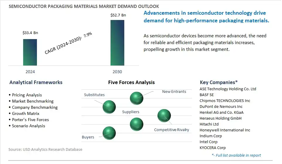
The global Semiconductor Packaging Materials Market is poised to register a 7.9% CAGR from $33.4 Billion in 2024 to $52.7 Billion in 2030.
The global Semiconductor Packaging Materials Market Study analyzes and forecasts the market size across 6 regions and 24 countries for diverse segments -By Material (Organic substrates, Lead frames, Bonding wires, Ceramic packages, Others), By End-User (Consumer electronics, Automotive, Medical devices, Communication and telecom, Others).
An Introduction to Global Semiconductor Packaging Materials Market in 2024
The semiconductor packaging materials market is experiencing robust growth driven by the increasing demand for advanced semiconductor devices in electronics, telecommunications, automotive, and industrial applications. Key trends shaping the future of the industry include the rising adoption of advanced packaging technologies such as flip-chip, wafer-level packaging, and system-in-package (SiP) to meet the performance, miniaturization, and reliability requirements of next-generation semiconductor devices. Moreover, there's a growing emphasis on materials innovation and compatibility with emerging packaging processes, including low-k dielectrics, copper interconnects, and lead-free solder alloys, to address challenges such as heat dissipation, signal integrity, and environmental sustainability. Additionally, advancements in substrate materials, underfill encapsulants, and die attach adhesives are driving innovation in semiconductor packaging materials, enabling manufacturers to enhance device performance, reduce form factor, and improve reliability while meeting cost and time-to-market requirements, thereby fueling market growth and competitiveness in the global semiconductor packaging materials market.
Semiconductor Packaging Materials Market Competitive Landscape
The market report analyses the leading companies in the industry including ASE Technology Holding Co. Ltd, BASF SE, Chipmos TECHNOLOGIES Inc, DuPont de Nemours Inc, Henkel AG and Co. KGaA, Heraeus Holding GmbH, Hitachi Ltd, Honeywell International Inc, Indium Corp, Intel Corp, KYOCERA Corp, LG Innotek Co. Ltd, MITSUI and CO. Ltd, Nan Ya Printed Circuit Board Corp, Nippon Steel Corp, Powertech Technology Inc, Samsung Electronics Co. Ltd, Taiwan Semiconductor Co. Ltd, Texas Instruments Inc.
Semiconductor Packaging Materials Market Dynamics
Semiconductor Packaging Materials Market Trend: Miniaturization and Advanced Packaging Technologies
A prominent market trend in semiconductor packaging materials is the trend towards miniaturization and the adoption of advanced packaging technologies driven by the demand for smaller, faster, and more power-efficient electronic devices. As consumer electronics, automotive electronics, and industrial applications continue to evolve, there is a growing need for semiconductor packages that can accommodate increasingly complex integrated circuits (ICs) while meeting stringent performance, reliability, and thermal management requirements. Advanced packaging technologies such as system-in-package (SiP), 2.5D and 3D packaging, wafer-level packaging (WLP), and fan-out wafer-level packaging (FOWLP) enable the integration of multiple chips, sensors, and passive components into compact and high-density packages, allowing manufacturers to achieve greater functionality and performance in smaller form factors. This trend is driving innovation in semiconductor packaging materials to support the development of next-generation electronic devices with enhanced functionality and performance.
Semiconductor Packaging Materials Market Driver: Technological Advancements in Semiconductor Manufacturing
The market for semiconductor packaging materials is being driven by technological advancements in semiconductor manufacturing processes and materials, including the development of new materials, processes, and assembly techniques to meet the evolving requirements of advanced semiconductor packaging applications. With the continuous advancement of semiconductor technologies such as microelectromechanical systems (MEMS), radio-frequency (RF) devices, power semiconductors, and optoelectronic devices, there is a growing demand for packaging materials that offer superior electrical, thermal, mechanical, and reliability performance. Additionally, advancements in materials science and nanotechnology are enabling the development of novel packaging materials with tailored properties such as low dielectric constant (low-k) dielectrics, high thermal conductivity substrates, and advanced interconnect materials. These technological advancements drive the adoption of new packaging materials and processes, enabling manufacturers to achieve higher levels of integration, performance, and reliability in semiconductor packages.
Semiconductor Packaging Materials Market Opportunity: Sustainable and Eco-Friendly Packaging Solutions
A potential opportunity for the semiconductor packaging materials market lies in the development of sustainable and eco-friendly packaging solutions to address environmental concerns and regulatory requirements for reducing electronic waste (e-waste) and minimizing the environmental impact of semiconductor manufacturing processes. As the electronics industry faces increasing scrutiny over its environmental footprint, there is a growing demand for green packaging materials and manufacturing practices that minimize resource consumption, energy usage, and waste generation throughout the product lifecycle. Manufacturers have an opportunity to innovate and offer sustainable packaging solutions such as bio-based polymers, recyclable materials, and environmentally friendly processes for semiconductor packaging. By embracing sustainability as a key driver of innovation, semiconductor packaging material suppliers can differentiate their products, meet the evolving needs of environmentally conscious customers, and contribute to the industry's transition towards a more sustainable and circular economy.
Semiconductor Packaging Materials Market Share Analysis: The Organic substrates segment generated the highest revenue in 2024
The Organic substrates segment is the largest in the Semiconductor Packaging Materials Market. organic substrates, such as printed circuit boards (PCBs) and laminate substrates, serve as the foundation for semiconductor packaging, providing structural support and electrical connections for integrated circuits (ICs) and other semiconductor devices. The widespread adoption of organic substrates is driven by their cost-effectiveness, lightweight nature, and compatibility with high-density packaging technologies such as flip-chip and chip-scale packaging. Additionally, organic substrates offer excellent thermal performance, allowing for efficient heat dissipation during semiconductor operation. Further, advancements in organic substrate materials and manufacturing processes have enhanced their performance and reliability, making them indispensable in various semiconductor packaging applications across industries such as consumer electronics, automotive, telecommunications, and computing. Over the forecast period, these factors contribute to the dominance of the Organic Substrates segment in the Semiconductor Packaging Materials Market.
Semiconductor Packaging Materials Market Share Analysis: The Automotive segment is poised to register the fastest growth rate (CAGR) over the forecast period to 2030
The Automotive segment is the fastest-growing segment in the Semiconductor Packaging Materials Market. The automotive industry is undergoing a significant transformation with the advent of electric vehicles (EVs), autonomous driving technologies, and connected vehicles. These technological advancements require sophisticated semiconductor components with higher performance, reliability, and miniaturization, driving the demand for advanced packaging materials. Additionally, the increasing adoption of electronic systems in modern vehicles for functions such as infotainment, advanced driver assistance systems (ADAS), and electrification further fuels the demand for semiconductor packaging materials. Further, stringent safety and quality standards in the automotive sector necessitate robust and reliable packaging solutions to ensure the integrity and longevity of electronic components in harsh operating environments. Furthermore, the growing trend towards electric and hybrid vehicles presents new opportunities for semiconductor packaging materials, particularly in power electronics and battery management systems. Over the forecast period, the Automotive segment experiences rapid growth in the Semiconductor Packaging Materials Market due to the increasing integration of semiconductor technologies in next-generation vehicles and the evolving automotive landscape.
Semiconductor Packaging Materials Market Share Analysis: The Communication and telecom segment is poised to register the fastest growth rate (CAGR) over the forecast period to 2030
The Communication and telecom segment is the fastest-growing segment in the Semiconductor Packaging Materials Market. The rapid expansion of communication networks, driven by advancements in technologies such as 5G, IoT (Internet of Things), and cloud computing, is driving the demand for high-performance semiconductor devices and components. These technologies require advanced semiconductor packaging materials capable of meeting stringent requirements for speed, reliability, and miniaturization. Additionally, the proliferation of smartphones, tablets, wearables, and other connected devices further fuels the demand for semiconductor packaging materials in the communication and telecom sector. Further, the increasing adoption of artificial intelligence (AI), machine learning, and data analytics in communication networks and devices drives the need for advanced semiconductor packaging solutions to support the processing and transmission of large volumes of data efficiently. Furthermore, the ongoing digital transformation across industries and the demand for seamless connectivity contribute to the sustained growth of the Communication and Telecom segment in the Semiconductor Packaging Materials Market. Over the forecast period, these factors converge to make the Communication and Telecom segment the fastest-growing segment in the Semiconductor Packaging Materials Market.
Semiconductor Packaging Materials Market Report Segmentation
By Material
Organic substrates
Lead frames
Bonding wires
Ceramic packages
Others
By End-User
Consumer electronics
Automotive
Medical devices
Communication and telecom
Others
Regions Included
North America (US, Canada, Mexico)
Europe (Germany, UK, France, Spain, Italy, Russia, Rest of Europe)
Asia Pacific (China, India, Japan, South Korea, Australia, South East Asia, Rest of Asia)
South America (Brazil, Argentina, Rest of South America)
Middle East and Africa (Saudi Arabia, UAE, Rest of Middle East, South Africa, Egypt, Rest of Africa)
Semiconductor Packaging Materials Companies Profiled in the Market Study
ASE Technology Holding Co. Ltd
BASF SE
Chipmos TECHNOLOGIES Inc
DuPont de Nemours Inc
Henkel AG and Co. KGaA
Heraeus Holding GmbH
Hitachi Ltd
Honeywell International Inc
Indium Corp
Intel Corp
KYOCERA Corp
LG Innotek Co. Ltd
MITSUI and CO. Ltd
Nan Ya Printed Circuit Board Corp
Nippon Steel Corp
Powertech Technology Inc
Samsung Electronics Co. Ltd
Taiwan Semiconductor Co. Ltd
Texas Instruments Inc
*- List Not Exhaustive
TABLE OF CONTENTS
1 Introduction to 2024 Semiconductor Packaging Materials Market
1.1 Market Overview
1.2 Quick Facts
1.3 Scope/Objective of the Study
1.4 Market Definition
1.5 Countries and Regions Covered
1.6 Units, Currency, and Conversions
1.7 Industry Value Chain
2 Research Methodology
2.1 Market Size Estimation
2.2 Sources and Research Methodology
2.3 Data Triangulation
2.4 Assumptions and Limitations
3 Executive Summary
3.1 Global Semiconductor Packaging Materials Market Size Outlook, $ Million, 2021 to 2030
3.2 Semiconductor Packaging Materials Market Outlook by Type, $ Million, 2021 to 2030
3.3 Semiconductor Packaging Materials Market Outlook by Product, $ Million, 2021 to 2030
3.4 Semiconductor Packaging Materials Market Outlook by Application, $ Million, 2021 to 2030
3.5 Semiconductor Packaging Materials Market Outlook by Key Countries, $ Million, 2021 to 2030
4 Market Dynamics
4.1 Key Driving Forces of Semiconductor Packaging Materials Industry
4.2 Key Market Trends in Semiconductor Packaging Materials Industry
4.3 Potential Opportunities in Semiconductor Packaging Materials Industry
4.4 Key Challenges in Semiconductor Packaging Materials Industry
5 Market Factor Analysis
5.1 Value Chain Analysis
5.2 Competitive Landscape
5.2.1 Global Semiconductor Packaging Materials Market Share by Company (%), 2023
5.2.2 Product Offerings by Company
5.3 Porter’s Five Forces Analysis
5.4 Pricing Analysis and Outlook
6 Growth Outlook Across Scenarios
6.1 Growth Analysis-Case Scenario Definitions
6.2 Low Growth Scenario Forecasts
6.3 Reference Growth Scenario Forecasts
6.4 High Growth Scenario Forecasts
7 Global Semiconductor Packaging Materials Market Outlook by Segments
7.1 Semiconductor Packaging Materials Market Outlook by Segments, $ Million, 2021- 2030
By Material
Organic substrates
Lead frames
Bonding wires
Ceramic packages
Others
By End-User
Consumer electronics
Automotive
Medical devices
Communication and telecom
Others
8 North America Semiconductor Packaging Materials Market Analysis and Outlook To 2030
8.1 Introduction to North America Semiconductor Packaging Materials Markets in 2024
8.2 North America Semiconductor Packaging Materials Market Size Outlook by Country, 2021-2030
8.2.1 United States
8.2.2 Canada
8.2.3 Mexico
8.3 North America Semiconductor Packaging Materials Market size Outlook by Segments, 2021-2030
By Material
Organic substrates
Lead frames
Bonding wires
Ceramic packages
Others
By End-User
Consumer electronics
Automotive
Medical devices
Communication and telecom
Others
9 Europe Semiconductor Packaging Materials Market Analysis and Outlook To 2030
9.1 Introduction to Europe Semiconductor Packaging Materials Markets in 2024
9.2 Europe Semiconductor Packaging Materials Market Size Outlook by Country, 2021-2030
9.2.1 Germany
9.2.2 France
9.2.3 Spain
9.2.4 United Kingdom
9.2.4 Italy
9.2.5 Russia
9.2.6 Norway
9.2.7 Rest of Europe
9.3 Europe Semiconductor Packaging Materials Market Size Outlook by Segments, 2021-2030
By Material
Organic substrates
Lead frames
Bonding wires
Ceramic packages
Others
By End-User
Consumer electronics
Automotive
Medical devices
Communication and telecom
Others
10 Asia Pacific Semiconductor Packaging Materials Market Analysis and Outlook To 2030
10.1 Introduction to Asia Pacific Semiconductor Packaging Materials Markets in 2024
10.2 Asia Pacific Semiconductor Packaging Materials Market Size Outlook by Country, 2021-2030
10.2.1 China
10.2.2 India
10.2.3 Japan
10.2.4 South Korea
10.2.5 Indonesia
10.2.6 Malaysia
10.2.7 Australia
10.2.8 Rest of Asia Pacific
10.3 Asia Pacific Semiconductor Packaging Materials Market size Outlook by Segments, 2021-2030
By Material
Organic substrates
Lead frames
Bonding wires
Ceramic packages
Others
By End-User
Consumer electronics
Automotive
Medical devices
Communication and telecom
Others
11 South America Semiconductor Packaging Materials Market Analysis and Outlook To 2030
11.1 Introduction to South America Semiconductor Packaging Materials Markets in 2024
11.2 South America Semiconductor Packaging Materials Market Size Outlook by Country, 2021-2030
11.2.1 Brazil
11.2.2 Argentina
11.2.3 Rest of South America
11.3 South America Semiconductor Packaging Materials Market size Outlook by Segments, 2021-2030
By Material
Organic substrates
Lead frames
Bonding wires
Ceramic packages
Others
By End-User
Consumer electronics
Automotive
Medical devices
Communication and telecom
Others
12 Middle East and Africa Semiconductor Packaging Materials Market Analysis and Outlook To 2030
12.1 Introduction to Middle East and Africa Semiconductor Packaging Materials Markets in 2024
12.2 Middle East and Africa Semiconductor Packaging Materials Market Size Outlook by Country, 2021-2030
12.2.1 Saudi Arabia
12.2.2 UAE
12.2.3 Oman
12.2.4 Rest of Middle East
12.2.5 Egypt
12.2.6 Nigeria
12.2.7 South Africa
12.2.8 Rest of Africa
12.3 Middle East and Africa Semiconductor Packaging Materials Market size Outlook by Segments, 2021-2030
By Material
Organic substrates
Lead frames
Bonding wires
Ceramic packages
Others
By End-User
Consumer electronics
Automotive
Medical devices
Communication and telecom
Others
13 Company Profiles
13.1 Company Snapshot
13.2 SWOT Profiles
13.3 Products and Services
13.4 Recent Developments
13.5 Financial Profile
ASE Technology Holding Co. Ltd
BASF SE
Chipmos TECHNOLOGIES Inc
DuPont de Nemours Inc
Henkel AG and Co. KGaA
Heraeus Holding GmbH
Hitachi Ltd
Honeywell International Inc
Indium Corp
Intel Corp
KYOCERA Corp
LG Innotek Co. Ltd
MITSUI and CO. Ltd
Nan Ya Printed Circuit Board Corp
Nippon Steel Corp
Powertech Technology Inc
Samsung Electronics Co. Ltd
Taiwan Semiconductor Co. Ltd
Texas Instruments Inc
14 Appendix
14.1 Customization Offerings
14.2 Subscription Services
14.3 Related Reports
14.4 Publisher Expertise
By Material
Organic substrates
Lead frames
Bonding wires
Ceramic packages
Others
By End-User
Consumer electronics
Automotive
Medical devices
Communication and telecom
Others
Countries Analyzed
North America (US, Canada, Mexico)
Europe (Germany, UK, France, Spain, Italy, Russia, Rest of Europe)
Asia Pacific (China, India, Japan, South Korea, Australia, South East Asia, Rest of Asia)
South America (Brazil, Argentina, Rest of South America)
Middle East and Africa (Saudi Arabia, UAE, Rest of Middle East, South Africa, Egypt, Rest of Africa)