Market Overview: Advanced Packaging Market to Reach $114 Billion by 2034 as AI Chip Demand Drives CoWoS, Heterogeneous Integration, and 3D Packaging Technologies
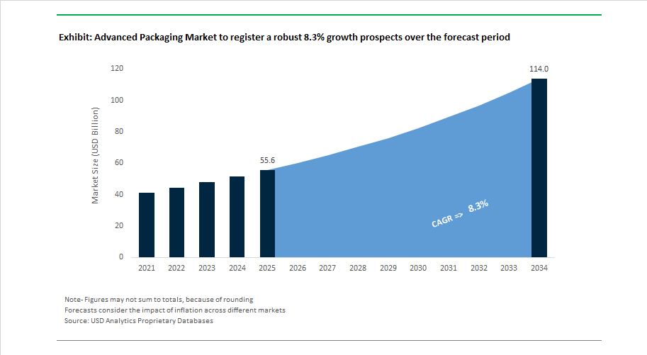
The global advanced packaging market is projected to grow from $55.6 billion in 2025 to $114 billion by 2034, registering a robust 8.3% CAGR fueled by explosive demand for AI accelerators, high-performance computing (HPC), data center processors, and next-generation memory architectures. Advanced packaging technologies including CoWoS (Chip-on-Wafer-on-Substrate), Fan-Out Wafer Level Packaging (FOWLP), High-Density Fan-Out (HDFO), 2.5D interposers, 3D IC stacking, hybrid bonding, chiplets, and advanced substrates are becoming central to semiconductor performance scaling as transistor-level advances slow. The market is shifting from traditional back-end assembly to system-level integration where packaging defines bandwidth, power efficiency, and thermal management. Capital expenditure by foundries, OSATs, and IDM players indicates structural capacity expansion to address supply constraints in AI chip packaging.
Strategic collaboration intensified in October 2024 when Amkor Technology and TSMC expanded their Arizona partnership to deliver turnkey CoWoS and InFO packaging services in the United States. Capacity reservation pressures emerged in August 2025 as Nvidia secured about 60% of global CoWoS wafer capacity for 2026, with additional allocations booked by Broadcom and Marvell Technology for custom AI ASICs serving hyperscale cloud providers. China strengthened domestic capabilities in November 2025 when SMIC opened a dedicated advanced packaging research institute focused on heterogeneous integration. Substrate innovation advanced in late 2025 as Intel and SKC reported pilot production progress for glass substrates aimed at higher routing density and dimensional stability. Architectural breakthroughs continued in December 2025 when Intel introduced its Z-Angle Memory prototype integrating memory within the processor package.
Capacity expansion accelerated in January 2026 as Intel shipped first 18A-node products using Foveros 3D stacking, while India cleared $4.6 billion in semiconductor projects to build OSAT and advanced packaging capability in Gujarat. In February 2026, TSMC approved a record $44.96 billion CapEx plan for 2026, allocating a substantial portion to advanced packaging and mask production. The same month, Samsung Electronics introduced HBM4 memory using hybrid copper bonding to increase interconnect density, and Amkor Technology announced a $2.5 to $3 billion investment plan targeting Arizona packaging facilities and HDFO ramp-up. ASE Technology projected LEAP advanced packaging revenue to double in 2026 as facilities operate near full utilization to serve AI processor demand. These developments confirm advanced packaging as a strategic bottleneck and a primary enabler of AI semiconductor scaling.
Strategic Market Trends and High-Value Opportunities Reshaping the Advanced Packaging Market
Market Trend: Semiconductor Packaging Shifts Toward Chiplet-Based Modular Integration
A fundamental inflection point is emerging as the industry departs from monolithic SoCs and pivots to chiplet architectures, where multiple dies with different process nodes are integrated within a unified package. The growing adoption of UCIe (Universal Chiplet Interconnect Express) as an open interoperability standard is making this transition commercially viable.
The release of UCIe 3.0 in August 2025 introduced support for 48 GT/s and 64 GT/s signalling, dramatically improving bandwidth density while reducing power-per-bit. Demonstrations at the OCP Global Summit showed how chiplet-enabled systems can integrate 3nm logic CPUs, GPU accelerators, memory, and signal-processing dies in modular Lego-like configurations. This shift is particularly relevant for AI infrastructure, where the cost of leading-edge monolithic silicon is no longer economically sustainable due to low yield rates at advanced nodes. Chiplets enable manufacturers to combine 3nm logic with more affordable 7nm or 10nm I/O dies, unlocking cost efficiencies while maintaining performance scaling.
Market Trend: National Industrial Policies Trigger Large-Scale Onshoring for Packaging Capacity
A global race to secure semiconductor sovereignty is accelerating the construction of advanced packaging megasites in the United States and Europe. Packaging had historically been outsourced to Asia even when chipmaking occurred domestically. That gap is now being aggressively reversed.
In January 2025, the U.S. Department of Commerce finalized USD 1.4 billion in direct awards under the National Advanced Packaging Manufacturing Program (NAPMP). Beneficiaries include Absolics, focused on glass-core substrates in Georgia, and Applied Materials, developing 3D silicon-core integration lines in California. Simultaneously, Amkor Technology’s USD 7 billion Peoria, Arizona campus marks one of the largest packaging-buildouts globally and directly services chips produced at TSMC’s U.S. fabs.
Europe is pursuing a parallel model. The European Commission granted Integrated Production Facility (IPF) status to the TSMC-Bosch-Infineon-NXP joint venture in Germany, enabling regulatory fast-track and permitting prioritization. These projects reflect a long-term vision to double Europe’s semiconductor value share by 2030, positioning packaging capability as essential to meeting that target.
Market Opportunity: Backside Power Delivery and Sub-2nm Node Enablement Through 3D Advanced Packaging
As transistor scaling encounters physical constraints at two nanometers and below, packaging becomes the mechanism through which Moore’s Law continues. Sub-2nm logic requires Backside Power Delivery (BSPD), where electrical routing is moved beneath the transistor layer to eliminate noise and improve switching speeds.
Intel’s 18A (1.8nm) technology moved into high-volume manufacturing in Q4 2025, marking the first commercial deployment of PowerVia BSPD combined with RibbonFET Gate-All-Around structures. Early performance disclosures indicate 15% more performance per watt, or alternatively 38% lower energy use at constant performance. Advanced packaging methods such as TSMC CoWoS-L, Intel Foveros, and wafer-to-wafer hybrid bonding are being redesigned to integrate BSPD into multi-die stacks. TSMC forecasts System-on-Integrated-Chip (SoIC) 3D packaging capacity to expand at triple-digit CAGR through 2026, primarily to meet AI workloads that require stacked memory, compute tiles, and high-speed interposer connectivity.
Market Opportunity: Automotive-Grade High-Bandwidth Packaging for Central Compute and Software-Defined Vehicles
Automotive electronics are evolving toward centralized vehicle compute platforms, where a single multi-die package powers advanced driver assistance, autonomous decision-making, infotainment, and sensor fusion. Packaging must therefore deliver data-center-level bandwidth while meeting AEC-Q100 Grade 2 qualification for temperature and vibration durability.
The imec Automotive Chiplet Program expanded to 14 multinational OEM and Tier-1 participants, including BMW, Bosch, Porsche, and Arm, to establish qualification standards and reliability testing methodologies. Thermo-mechanical stress testbeds now enable validation of chiplet-based systems up to 105°C ambient, simulating long-term vehicle use.
Meanwhile, updated AEC Q100-010 and Q007 reliability standards (2025) explicitly address material-stress and shear-risk issues tied to large-form-factor, high-bandwidth chip packages used in electric vehicles. As EVs evolve into rolling edge-compute platforms, high-bandwidth advanced packaging becomes a mission-critical enabler for safety-certified autonomous systems, opening a profitable niche for vendors capable of guaranteeing thermal reliability, delamination resistance, and field lifetime operation.
Advanced packaging is now inseparable from chip performance, semiconductor sovereignty, AI scalability, and EV platform design. Suppliers positioned with UCIe-ready chiplet technology, domestic packaging capacity, BSPD integration capability, and automotive-grade reliability validation will define the competitive hierarchy of the global semiconductor ecosystem through 2030.
Advanced Packaging Market Share and Segmentation Insights
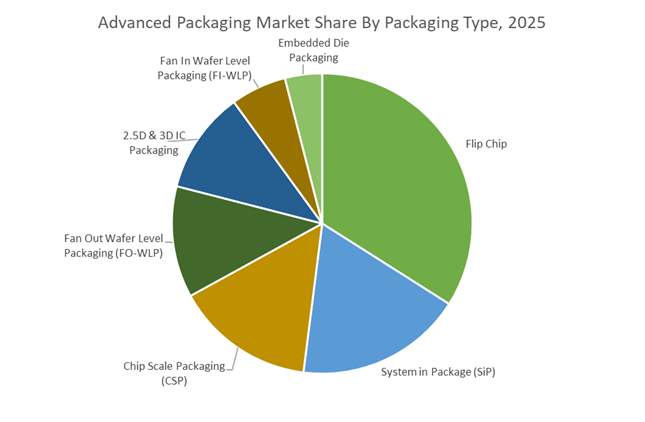
Market Share by Packaging Type: Flip Chip Leads While 2.5D/3D IC Drives Structural Growth
Flip Chip holds approximately 34% of the advanced packaging market in 2025, retaining leadership as the incumbent solution for high-pin-count CPUs, GPUs, and application processors. Although mature, its lifecycle is being extended through Flip Chip Ball Grid Array adoption in AI server chips and copper hybrid bonding in premium designs, lifting average selling prices. System in Package ranks second and dominates mobile and wearables, offering rapid heterogeneous integration of RF, memory, and sensors without silicon interposers. 2.5D & 3D IC packaging is the fastest-growing segment, powered by High Bandwidth Memory stacking for AI accelerators, where capacity is constrained at the packaging level rather than wafer fabs. Fan Out WLP has stabilized as the mobile standard, with cautious migration toward panel-level formats. Embedded die packaging remains smallest due to complexity but is gaining traction in high-reliability automotive and aerospace power modules.
Market Share by End-Use Industry: Consumer Electronics Leads Volume as HPC Becomes the Profit Engine
Consumer electronics account for roughly 37% of advanced packaging demand in 2025, driven by smartphones and wearables consuming large volumes of Flip Chip, SiP, and CSP, though growth has slowed to low single digits. High performance computing and data centers represent the primary growth and margin driver, consuming the most advanced 2.5D/3D and fan-out architectures for AI training, inference, and hyperscale cloud workloads, making advanced packaging a bottleneck across the AI supply chain. Automotive is rising from a low base as ADAS, infotainment, and sensor fusion increase usage of Flip Chip and FO-WLP, though safety-grade reliability limits rapid 3D IC adoption. Telecommunications growth is moderating as 5G rollouts mature, while aerospace and defense remain small but command premium pricing. Industrial and medical devices adopt CSP and SiP gradually, constrained by regulatory timelines.
Competitive Landscape: Chiplet Architectures and Heterogeneous Integration Redefining the Advanced Packaging Market
The Advanced Packaging Market is being reshaped by AI acceleration, chiplet-based design, and heterogeneous integration as leading OSATs and foundries race to overcome Moore’s Law limitations. Competitive advantage now hinges on high-density fan-out, 2.5D/3D stacking, wafer-level multi-chip modules, and hybrid bonding. Market leaders are aggressively expanding capacity across Taiwan, Malaysia, China, and the United States while integrating packaging directly with logic and memory fabrication. Advanced packaging has become a strategic differentiator for AI GPUs, HBM integration, automotive electronics, and edge computing, with capital intensity and ecosystem control defining long-term leadership.
ASE Technology Holding Co., Ltd. scales VIPack™ platforms to power global chiplet adoption
ASE Technology Holding is the world’s largest OSAT provider and a primary manufacturing backbone for chiplet-based architectures. In February 2026, ASE confirmed its advanced packaging business is on track to double to $3.2 billion by year-end, driven by foundry spillover demand. Its VIPack™ umbrella covers high-density fan-out, 2.5D/3D integration, and System-in-Package solutions. Subsidiary Siliconware Precision Industries has become a Tier-1 supplier for NVIDIA AI GPU packaging. ASE’s 2026 CapEx prioritizes High-Density Fan-Out expansion in Malaysia and Taiwan to support decentralized AI and edge computing workloads.
TSMC integrates silicon fabrication with CoWoS® and SoIC packaging leadership
TSMC has redefined the foundry model by embedding advanced packaging directly into wafer fabrication, creating a true one-stop platform for hyperscale AI customers. Its proprietary CoWoS® and SoIC technologies remain the gold standard for HBM-to-logic integration. During 2025–2026, TSMC scaled System-on-Wafer to enable wafer-scale AI processing. The AP7 facility in Chiayi is scheduled for high-volume output in 2026, targeting wafer-level multi-chip modules. Strategically, TSMC is transitioning toward CoPoS to boost chips-per-panel and effectively double throughput by 2027–2028, reinforcing dominance in next-generation AI packaging.
Amkor Technology, Inc. anchors U.S. advanced packaging with automotive and 5G specialization
Amkor Technology is the leading U.S.-based OSAT, playing a central role in semiconductor onshoring. The company reported $6.71 billion in 2025 revenue, with Flip Chip and wafer-level products contributing 83%. Amkor is constructing a major advanced packaging facility in Arizona to support nearby leading-edge fabs. It holds strong positions in automotive ADAS and 5G RF modules while advancing H-Series high-density fan-out, enabling fast chip-to-chip links without silicon interposers. This combination of domestic manufacturing, automotive reliability, and HDFO integration positions Amkor as a critical backend partner for U.S. semiconductor supply chains.
Intel Corporation leverages EMIB and Foveros to launch its foundry renaissance
Intel Corporation is repositioning itself as a major foundry by using advanced packaging as its competitive wedge. EMIB and Foveros enable cost-efficient multi-die interconnects and 3D stacking, offering alternatives to interposer-heavy approaches. In late 2025, Intel attracted customers including Apple, Qualcomm, and NVIDIA for EMIB services. The debut of EMIB 3.5D allows massive silicon assemblies beyond reticle limits. Intel’s strategy ties packaging directly to its 18A node, enabling customers to mix chiplets from multiple foundries within Intel-packaged systems.
JCET Group accelerates edge intelligence with ultra-high-density fan-out
JCET Group is Mainland China’s leading OSAT, targeting edge intelligence and high-density integration. The company posted RMB 18.61 billion in H1 2025 revenue, with computing-related sales up 72% year-over-year on AI server demand. JCET strengthened storage capabilities through the integration of SanDisk China, expanding leadership in NAND and SSD packaging. Its XDFOI™ technology addresses chiplet-based HPC and 5G/6G use cases. Automotive electronics is a major growth driver, with nearly 40% expansion in 2025 supported by specialized EV power module packaging and localized manufacturing scale.
Samsung Electronics unifies memory, logic, and packaging for AI acceleration
Samsung Electronics stands apart with in-house memory, foundry, and advanced packaging capabilities. In early 2026, Samsung began mass production of 3D-stacked logic-on-logic SoCs, bypassing conventional scaling limits. Its I-Cube and X-Cube platforms are optimized for integrating HBM3e and HBM4. Samsung is advancing hybrid bonding to sub-10-micron pitch, dramatically increasing interconnect density and bandwidth. This internal synergy allows Samsung to design, fabricate, and package complete AI accelerators faster than competitors dependent on multi-vendor coordination, reinforcing its strategic position in high-performance computing and AI infrastructure.
Malaysia Advanced Packaging Market: From OSAT Backbone to Global 3D Packaging Powerhouse
Malaysia has transitioned from a traditional assembly base into one of the world’s most strategically important advanced packaging hubs. In December 2025, the Malaysian government confirmed that Intel plans to invest an additional $208 million to further anchor the country as its global assembly and test operations center. This follows Intel’s $2.9 billion advanced packaging facility in Penang, which reached 99% completion by late 2025 and will be the first site outside the United States to deploy Foveros 3D packaging technology at scale.
The country’s role is expanding rapidly through parallel investments. Intel’s internal “Pelican” project in Penang and “Falcon” project in Kulim are under construction and are expected to deliver output through 2026, focusing on EMIB and advanced 3D IC packaging. Malaysia already accounts for approximately 13% of the global OSAT market, according to the Prime Minister’s 2025 industrial report. Capacity was further strengthened when ASE Technology Holding launched its fifth Penang facility in February 2025. Workforce readiness is being addressed under the National Industrial Master Plan 2030, which integrates digital twin simulation, automated material handling, and semiconductor-specific talent pipelines, positioning Malaysia as a long-term advanced packaging anchor.
Taiwan Advanced Packaging Market: Hyper-Scaling CoWoS and SoIC for the AI Compute Era
Taiwan remains the global epicenter of advanced packaging innovation, driven by aggressive capacity scaling to meet AI accelerator demand. At the 2025 Technology Symposium, TSMC announced plans to construct nine new facilities in a single year, including a dedicated advanced packaging plant. Central to this expansion is CoWoS technology, with monthly capacity targeted to rise from roughly 80,000 wafers to 130,000 wafers by the end of 2026.
Next-generation integration is accelerating. Equipment move-in at the AP8 facility in the Southern Taiwan Science Park and the AP7 facility in Chiayi began in late 2025, with a sharp focus on SoIC technology that is projected to grow at a CAGR exceeding 100% through 2026. TSMC’s Kaohsiung expansion includes five fabs supporting A16 and more advanced nodes, all of which rely on ultra-high-density 3D stacking. Taiwan-based OSATs are simultaneously advancing hybrid bonding to support vertical stacking for Blackwell-generation GPUs and future AI accelerators. Regulatory scrutiny is increasing as well, with Taiwanese authorities launching trade secret investigations in November 2025 following executive movements across top-tier foundry and packaging firms.
United States Advanced Packaging Market: CHIPS-Driven Reindustrialization of Advanced Packaging
The United States is rebuilding domestic advanced packaging leadership through coordinated federal funding and private investment. In January 2025, the U.S. Department of Commerce finalized $1.4 billion in awards under the CHIPS National Advanced Packaging Manufacturing Program, accelerating onshore capability development. A flagship example is Amkor Technology’s $2 billion advanced packaging and test campus in Peoria, Arizona, which broke ground in late 2025 and is expected to generate 2,000 high-skilled jobs.
Memory and substrate innovation are core pillars. SK hynix is investing $3.87 billion in West Lafayette, Indiana, to establish an advanced packaging fabrication and R and D site for AI-centric memory products. Substrate leadership is being addressed through awards to Absolics and Applied Materials, each receiving $100 million to advance glass-core and silicon-core substrate technologies for heterogeneous integration. Academic commercialization is also critical, with Arizona State University securing $100 million to scale 600 mm panel-level manufacturing and fan-out wafer-level processing, bridging lab innovation and industrial deployment.
Japan Advanced Packaging Market: State-Orchestrated Revival of a Full-Stack Packaging Ecosystem
Japan is executing a state-backed strategy to reestablish a complete domestic semiconductor supply chain with advanced packaging at its core. In March 2025, the government allocated an additional ¥802.5 billion to the startup Rapidus, including ¥127 billion earmarked specifically for back-end processing. Total taxpayer support for Rapidus has reached approximately ¥1.72 trillion, underscoring national commitment.
Rapidus aims to initiate pilot production of 2 nm chips in April 2025, with mass production planned for late 2027, a timeline that requires localized 2.5D and 3D packaging ecosystems. Japanese materials companies are pivoting toward non-conductive films and advanced underfills to support high-bandwidth memory integration. The “All-Japan” effort is reinforced by direct investments from Toyota, Sony, and SoftBank, focusing on AI-ready packaging components. Environmental leadership is also advancing, as updated economy ministry certifications promote carbon-neutral semiconductor packaging and alternative gas usage in back-end processes.
South Korea Advanced Packaging Market: One-Stop Integration and HBM-Centric Scaling
South Korea’s advanced packaging strategy is centered on vertical integration and memory leadership. Samsung Electronics emphasized in early 2026 that its competitive edge lies in delivering logic, memory, foundry, and advanced packaging as a unified solution. This approach is gaining traction as AI customers seek simplified supply chains.
Samsung is rapidly expanding I-Cube and X-Cube capacity as alternatives to CoWoS, addressing global supply tightness for AI accelerators. Advanced packaging is tightly linked to memory innovation, particularly HBM3E Shinebolt and upcoming HBM4, which require complex vertical stacking and thermal management now being scaled at Cheonan and Onyang. The company is also advancing SOCAMM2 modules to support on-device AI across infrastructure and mobile platforms. Government backing remains strong through the K-Chips Act, which provides tax credits for back-end semiconductor investments to preserve competitiveness against Taiwanese foundries.
Vietnam Advanced Packaging Market: Rapid Maturation from Assembly to System-Level Packaging
Vietnam has emerged as a high-growth advanced packaging location within Southeast Asia. In November 2025, Amkor Technology Vietnam received the Vietnam Semiconductor Distinguished Industry Award at SEMIExpo Vietnam, recognizing its role in transforming the national semiconductor landscape. Amkor’s Bac Ninh facility has become a major high-volume assembly and test site, while also hosting intensive technical bootcamps to build local engineering capabilities.
The ecosystem is deepening quickly. Vietnam has moved beyond basic assembly into advanced testing and system-level packaging, attracting suppliers of automated material handling systems and cleanroom equipment. Workforce transition is a key differentiator, with OSATs collaborating closely with local STEM universities to bridge the gap between academic research and high-volume commercialization. This model is positioning Vietnam as a scalable, cost-competitive node within global advanced packaging supply chains.
Strategic Positioning in the Advanced Packaging Industry
Advanced Packaging Market County Level Snapshot
|
Country
|
Strategic Focus
|
Competitive Impact
|
|
Malaysia
|
Foveros, EMIB, OSAT scale
|
Global assembly and 3D packaging hub
|
|
Taiwan
|
CoWoS, SoIC, A16 node support
|
AI-driven advanced packaging leadership
|
|
United States
|
CHIPS funding, substrates, panel-level tech
|
Reindustrialized back-end ecosystem
|
|
Japan
|
Rapidus-led 2 nm integration
|
State-backed full-stack revival
|
|
South Korea
|
HBM-centric vertical integration
|
One-stop AI packaging solutions
|
|
Vietnam
|
System-level packaging, talent scaling
|
Fast-maturing OSAT growth engine
|
Advanced Packaging Market Report Scope
Advanced Packaging Market
|
Parameter
|
Details
|
|
Market Size (2025)
|
$55.6 Billion
|
|
Market Size (2034)
|
$114 Billion
|
|
Market Growth Rate
|
8.3%
|
|
Segments
|
By Packaging Type (Flip Chip, Fan Out Wafer Level Packaging, Fan In Wafer Level Packaging, 2.5D and 3D IC Packaging, System in Package, Embedded Die Packaging, Chip Scale Packaging), By Integration Technology (Through Silicon Via, Chip on Wafer on Substrate, Fan Out on Substrate, Hybrid Bonding, Multi Die Integration), By End Use Industry (High Performance Computing and Data Centers, Consumer Electronics, Automotive, Telecommunications, Industrial and Medical Devices, Aerospace and Defense), By Component (Central Processing Units and Graphics Processing Units, High Bandwidth Memory, Baseband Processors and Modems, Power Management Integrated Circuits, Image Sensors)
|
|
Study Period
|
2019- 2025 and 2026-2034
|
|
Units
|
Revenue (USD)
|
|
Qualitative Analysis
|
Porter’s Five Forces, SWOT Profile, Market Share, Scenario Forecasts, Market Ecosystem, Company Ranking, Market Dynamics, Industry Benchmarking
|
|
Companies
|
ASE Technology Holding, Amkor Technology, Intel Corporation, Taiwan Semiconductor Manufacturing Company, Samsung Electronics, JCET Group, SK hynix, Siliconware Precision Industries, Powertech Technology, UTAC Group, Texas Instruments, Broadcom, Tongfu Microelectronics, Huatian Technology, Chipbond Technology Corporation
|
|
Countries
|
US, Canada, Mexico, Germany, France, Spain, Italy, UK, Russia, China, India, Japan, South Korea, Australia, South East Asia, Brazil, Argentina, Middle East, Africa
|
Advanced Packaging Market Segmentation
By Packaging Type
- Flip Chip
- Fan Out Wafer Level Packaging
- Fan In Wafer Level Packaging
- 2.5D and 3D IC Packaging
- System in Package
- Embedded Die Packaging
- Chip Scale Packaging
By Integration Technology
- Through Silicon Via
- Chip on Wafer on Substrate
- Fan Out on Substrate
- Hybrid Bonding
- Multi Die Integration
By End Use Industry
- High Performance Computing and Data Centers
- Consumer Electronics
- Automotive
- Telecommunications
- Industrial and Medical Devices
- Aerospace and Defense
By Component
- Central Processing Units and Graphics Processing Units
- High Bandwidth Memory
- Baseband Processors and Modems
- Power Management Integrated Circuits
- Image Sensors
By Region
- North America (United States, Canada, Mexico)
- Europe (Germany, France, United Kingdom, Spain, Italy, Rest of Europe)
- Asia Pacific (China, India, Japan, South Korea, Australia, Rest of APAC)
- South and Central America (Brazil, Argentina, Rest of SCA)
- Middle East and Africa (Saudi Arabia, UAE, South Africa, Rest of Middle East, Rest of Africa)
Top Companies in Advanced Packaging Industry
- ASE Technology Holding
- Amkor Technology
- Intel Corporation
- Taiwan Semiconductor Manufacturing Company
- Samsung Electronics
- JCET Group
- SK hynix
- Siliconware Precision Industries
- Powertech Technology
- UTAC Group
- Texas Instruments
- Broadcom
- Tongfu Microelectronics
- Huatian Technology
- Chipbond Technology Corporation
*- List not Exhaustive
