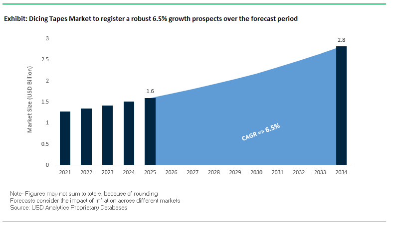
The global dicing tapes market is rapidly emerging as a structurally critical enabler of advanced semiconductor manufacturing, reflecting its direct impact on yield, uptime, and package reliability in back-end-of-line (BEOL) operations. The market is projected to expand from USD 1.6 billion in 2025 to USD 2.8 billion by 2034, at a 6.5% CAGR, driven by the industry-wide shift toward 3D integration, extreme wafer thinning, and high-density packaging architectures. As logic, memory, and heterogeneous integration platforms scale below the 10 nm node and adopt ultra-thin silicon, wafer singulation has become a yield-determining step rather than a peripheral process. This elevates dicing tapes from basic adhesion films to precision-engineered materials required to deliver controlled adhesion, electrostatic discharge (ESD) protection, and mechanical stability under increasingly fragile wafer conditions.
Demand is being reshaped by a clear structural shift in OEM behavior and packaging flows. Advanced nodes supporting AI accelerators, HPC processors, 5G devices, and autonomous electronics rely on UV-curable dicing tapes and integrated Dicing Die Attach Films (DDAF) to manage wafer thicknesses below 20 µm, maintain TSV compatibility, and reduce die loss during high-speed pick-up. Manufacturer-led material innovation has focused on dimensionally stable, residue-free, solvent-resistant, and ESD-controlled films, aligning with requirements observed across OSAT and foundry back-end lines. UV tapes capable of achieving up to 90% adhesive strength reduction after UV irradiation enable precise die release without contamination, while advanced anti-static formulations achieving surface voltages below 0.01 kV mitigate ESD risk in AI- and HPC-grade devices. These performance thresholds are no longer differentiators but baseline requirements for high-volume advanced packaging.
Integrated dicing and die attach systems are replacing legacy multi-step lamination, temporary bonding, and adhesive application workflows, directly reducing process complexity and cumulative defect risk. DDAF solutions improve bond line thickness (BLT) uniformity, support low-temperature bonding, and maintain adhesion integrity through solvent cleaning and TSV formation, addressing limitations inherent in conventional dicing tapes. At the same time, the adoption of eco-friendly, solvent-free, and low-VOC formulations reflects tightening environmental compliance across Asia, Europe, and North America without compromising thermal, mechanical, or chemical performance. These shifts connect material-level performance to business outcomes: higher singulation yield, reduced rework, improved throughput, and longer tool uptime. Looking forward, manufacturing strategies are converging around vertically integrated film systems, secure raw material sourcing, and compliance-ready adhesive chemistries, positioning dicing tape suppliers as long-term process partners rather than interchangeable material vendors in advanced semiconductor packaging ecosystems.
The dicing tapes industry is rapidly evolving to meet the needs of next-generation semiconductor packaging and heterogeneous integration. Key industry players are advancing R&D in UV-curable formulations, conductive die attach films, and solvent-resistant tapes, aligning with the shift toward high-performance computing (HPC), electric vehicles (EVs), and space-grade semiconductors.
In September 2025, Resonac Corporation (formerly Showa Denko Materials) announced the launch of the 27-member JOINT3 Consortium, in partnership with global electronics leaders. The initiative focuses on developing large-format panel-level interposers (515×510 mm), a move expected to redefine dicing and handling material requirements for expanded substrate dimensions. A few months earlier, in July 2025, Furukawa Electric reported significant progress on its C-DAF (Conductive Dicing Die Attach Film)—a breakthrough in heat-dissipating materials offering thermal conductivity exceeding 10 W/m·K, crucial for 5G and power electronics packaging.
Global trade and policy are also reshaping material strategies. August 2025 saw the introduction of new U.S. tariff measures, which disrupted raw material sourcing and cost structures for film manufacturers, especially those supplying adhesive components and UV-curable polymers. Simultaneously, eco-friendly material compliance is intensifying: April 2025 regulations have accelerated the transition toward low-VOC, hot-melt-based formulations, aligning with environmental policies across Asia and the EU.
Nitto Denko Corporation’s R&D milestone (March 2025) on solvent-resistant dicing tapes underscores industry readiness for ultra-thin wafer support during solvent cleaning in TSV and IGBT device manufacturing. Meanwhile, Lintec Corporation (February 2025) reinforced its leadership by promoting its Adwill UV and non-UV tape series alongside Wafer Mounting Systems and UV Irradiation Systems, offering end-to-end wafer processing ecosystems tailored for chiplet and SiP production lines.
Further, the growing influence of regional manufacturing expansions across Taiwan, South Korea, and China (May 2025) is creating competitive tension. Suppliers are racing to provide tapes with tensile uniformity and minimal warpage, meeting the mechanical precision required in memory and logic chip wafer singulation. In parallel, Resonac’s 2025 space-based evaluation program aboard the ISS validated its back-end materials for extreme-environment semiconductor applications, opening pathways for space and defense-grade wafer processing.
The semiconductor miniaturization trend is compelling the industry to adopt ultra-thin, high-adhesion UV-curable dicing tapes that can support wafer thinning below 50µm—a necessity for Fan-Out Wafer-Level Packaging (FO-WLP) and Chip-Scale Packages (CSPs). These advanced dicing materials must simultaneously provide strong initial adhesion during the dicing phase to prevent wafer cracking and ultra-low residual adhesion post UV-curing to enable smooth, damage-free die pick-up.
Recent material breakthroughs demonstrate that leading manufacturers have successfully launched integrated Dicing Die Attach Film (DDAF) solutions capable of maintaining wafer integrity during singulation and die bonding for 50µm-thin silicon wafers. These hybrid systems allow wafer mounting at low temperatures (as low as 40°C), preventing thermal deformation and mechanical stress on fragile wafers during high-precision cutting and assembly.
Performance specifications for next-generation UV-curable dicing tapes are highly demanding. For instance, standard UV-tape formulations exhibit initial peel adhesion between 2.80–3.30 N/10mm, which must be reduced to as low as 0.08–0.30 N/10mm after UV exposure. The precise control in adhesion transition ensures high-yield die singulation for small dies in wafer-level chip-scale packaging (WLCSP), minimizing die loss and increasing throughput in automated semiconductor assembly lines.
The global transition toward wide-bandgap semiconductors, notably Silicon Carbide (SiC) and Gallium Nitride (GaN)—is creating demand for high-durability dicing tapes capable of withstanding intense cutting conditions inherent to these materials. As power electronics, electric vehicles (EVs), and 5G/6G RF systems increasingly depend on SiC and GaN devices, the mechanical and thermal performance of dicing support materials has become a critical manufacturing constraint.
For SiC wafer dicing, which uses diamond blades spinning at 25,000–35,000 rpm with feed rates of 20–40 mm/s, the tape must maintain superior die fixation to prevent die shift, cracking, or contamination during the high-friction cutting process. These next-generation UV tapes are engineered for exceptional heat dissipation, solvent resistance, and thermal stability, ensuring adhesive performance remains consistent despite coolant flow exposure and localized frictional heat.
In advanced Stealth Dicing Before Grind (SDBG) and Through-Silicon Via (TSV) packaging flows, dicing tapes face harsh processing environments involving chemical cleaning and electroplating. Thus, tapes with solvent resistance and high pick-up reliability post-cleaning are crucial to maintain mechanical integrity throughout the back-end-of-line (BEOL) process. These innovations are positioning high-performance dicing tapes as indispensable for processing ultra-hard semiconductor substrates and achieving yield stability across new-generation wafer types.
The global semiconductor industry’s pivot toward Heterogeneous Integration (HI) and Chiplet-Based Packaging represents a major growth avenue for the dicing tapes market. As manufacturers move away from traditional monolithic chip architectures toward multi-die assemblies combining logic, memory, and I/O components, the demand for next-generation dicing tapes with tunable adhesion characteristics is rising sharply.
In these advanced packaging workflows, Dicing Die Attach Films (DDAF) and Integrated Dicing Die Bonding Tapes (IDDBT) are replacing traditional multi-step lamination and adhesive application processes. By combining the dicing support and die bonding functions into a single integrated solution, these materials eliminate die tilting, adhesive overflow, and rework issues.
For stacked-die assemblies—such as High Bandwidth Memory (HBM) or 3D logic integration—new DDAF products with controlled film thicknesses of 10–25µm provide exceptional bond-line uniformity and high-throughput lamination. These materials also support low-temperature bonding conditions, aligning with the shift toward thermally sensitive chiplet assembly lines. As semiconductor foundries and OSATs (Outsourced Semiconductor Assembly and Test companies) continue to scale HI production, integrated dicing-bonding tapes will become a cornerstone material for improving manufacturing yield and cost-efficiency.
As EV powertrain systems, renewable energy inverters, and high-frequency communication modules increasingly adopt compound semiconductors, demand is accelerating for UV-curable, high-temperature-resistant, and residue-free dicing tapes tailored to these next-generation materials. The opportunity extends beyond traditional silicon wafers to SiC, GaN, and Sapphire substrates, each requiring unique adhesion and release characteristics to prevent mechanical stress and thermal damage.
Dicing tape manufacturers are collaborating with semiconductor OEMs to develop specialized adhesive chemistries optimized for ultra-hard and thick wafers (up to 300µm) used in power module manufacturing. These high-adhesion films withstand laser-assisted dicing and grinding-before-dicing (GBD) processes without residue transfer, ensuring high-quality die surfaces critical for downstream bonding operations.
Further, the integration of UV-activated and heat-assisted release mechanisms is enabling faster, contamination-free die pick-up—an essential requirement for automated power module assembly. As EV adoption accelerates, these innovations offer a multi-billion-dollar growth opportunity for manufacturers supplying high-reliability dicing materials that support sustainable semiconductor production and high-yield power electronics fabrication.
Dicing Tapes Market Share Insights, 2025-2034
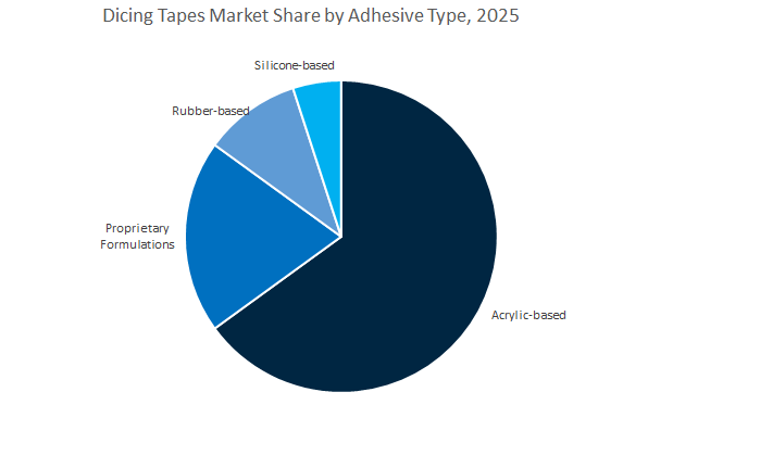
Acrylic-Based Adhesives Lead the Global Dicing Tapes Market with 62.6% Share Owing to Precision, Clean Processing, and Superior Releasability
Acrylic-based dicing tapes dominate the global dicing tapes industry, accounting for an estimated 62.6% share in 2025, due to their unmatched combination of controlled adhesion, optical clarity, and chemical stability. These tapes are the default choice for silicon wafer dicing, back grinding, and MEMS fabrication, offering superior mechanical stability during singulation while ensuring contamination-free processing—an essential requirement for semiconductor manufacturing. Their ability to maintain adhesion throughout mechanical or UV exposure steps, followed by clean release, makes them indispensable in high-throughput, automated wafer dicing operations. Moreover, UV-curable acrylic adhesives have become the industry benchmark for advanced packaging lines, allowing precise tuning of adhesion strength after exposure to ultraviolet light, ensuring defect-free die detachment. As wafer sizes increase and node geometries shrink, the demand for low-residue, ionic-contamination-free acrylic systems continues to grow. Their compatibility with 5G, AI, and high-density integrated circuit (IC) manufacturing cements acrylic-based dicing tapes as the cornerstone of modern semiconductor packaging workflows.
Proprietary Formulations Gain Momentum in Advanced Semiconductor Packaging and Ultra-Thin Wafer Processing
Proprietary adhesive formulations represent a high-value and rapidly expanding segment of the global dicing tapes market. These customized chemistries are designed to address next-generation packaging challenges, including ultra-thin wafer handling, chiplet integration, and heterogeneous packaging. Unlike standard tapes, proprietary systems can be engineered for specific substrate materials, temperature profiles, and post-dicing cleaning requirements, offering superior process control and yield. They are increasingly used in 3D NAND, fan-out wafer-level packaging (FOWLP), and system-in-package (SiP) technologies, where even minimal contamination or substrate stress can compromise performance. These formulations often leverage hybrid polymer systems with dual-cure mechanisms (UV + thermal) or nano-engineered surface modifiers to achieve high adhesion selectivity. Their premium pricing and adoption across Tier-1 fabs and OSATs (Outsourced Semiconductor Assembly and Test) make them a crucial growth engine for the market’s innovation trajectory.
Wafer Dicing Dominates the Market with 50.9% Share, Anchoring the Global Semiconductor Manufacturing Ecosystem
Wafer dicing remains the core and largest application of the global dicing tapes market, accounting for 50.9% of total demand in 2025. In this process, the tape plays a dual function—firmly holding the wafer during precision sawing operations while enabling easy die removal without cracking or chipping. With the semiconductor industry shifting toward advanced node manufacturing (below 7nm) and larger wafer formats (300mm and 450mm), the precision requirements for dicing tapes have intensified. UV-curable and heat-releasable tapes have become standard to ensure low-damage die singulation and high-speed pick-and-place automation. The segment’s dominance is reinforced by the exponential demand for chips used in smartphones, AI accelerators, automotive electronics, and IoT devices, all of which require exacting process reliability. Furthermore, the transition to compound semiconductors (SiC, GaN) in power electronics adds complexity, driving innovation in adhesive formulations optimized for hard substrates and high cutting loads. As a result, wafer dicing continues to be the technological and revenue backbone of the industry.
Back Grinding and Thinning Applications Gain Traction with the Surge in 3D Packaging and Advanced Node Integration
Back grinding (wafer thinning) is the second-largest and one of the fastest-growing applications, driven by the evolution toward 3D IC packaging and stacked die architectures. Dicing tapes used in this process must temporarily bond to the wafer’s front side, protecting active circuits during grinding and thinning before cleanly releasing without residue. This process is vital for enabling ultra-thin wafers (as thin as 25–50 µm) used in high-performance computing, mobile SoCs, and high-bandwidth memory (HBM). The growing use of UV-releasable tapes ensures stable adhesion during grinding, followed by controlled release under UV exposure to prevent die damage. The segment’s growth correlates strongly with the adoption of chiplet architectures and the increasing complexity of packaging technologies like 2.5D interposers and fan-out packaging. As semiconductor manufacturers pursue thinner, more thermally efficient chips, the back grinding application will continue to serve as a key technological enabler for next-generation microelectronics.
The global dicing tapes market is dominated by Japanese material science companies known for their precision adhesive formulations, ultra-thin film manufacturing, and integrated wafer processing solutions. Companies like Nitto Denko, Lintec, Resonac, Furukawa Electric, and Sumitomo Electric Fine Polymer lead through technology integration, R&D investment, and alignment with semiconductor megatrends such as miniaturization, thermal management, and advanced packaging automation.
Nitto Denko maintains a commanding presence in the wafer processing materials market, offering its ELEP HOLDER product series, which includes UV Release and Low Adhesion Release dicing tapes for ultra-thin wafer applications. The company’s innovation in Dicing Die Attach Film (DDAF) merges dicing and die attach functionalities into one process, streamlining semiconductor packaging while enhancing bond uniformity and yield. With ongoing R&D in solvent-resistant tapes for TSV and ultra-thin wafer handling, Nitto continues to define standards for dimensional stability and clean release in wafer singulation processes.
Lintec Corporation leads with its Adwill brand, encompassing UV-curable, back grinding, and dicing die bonding tapes. Its differentiation lies in offering both tape materials and complementary equipment systems like Wafer Mounting and UV Irradiation platforms, ensuring optimal process synchronization. Lintec’s Next Generation Innovation Group accelerates the adoption of advanced thin-film and adhesion control technologies, addressing the demands of SiP and heterogeneous integration manufacturing. With expertise across adhesion chemistry, coating, and surface modification, Lintec maintains a competitive edge in ESD control and precision bonding performance.
Resonac Corporation (formerly Showa Denko Materials) plays a strategic role in global semiconductor ecosystems through collaborative R&D and materials integration. As a founding member of the JOINT2 and JOINT3 consortia, Resonac co-develops materials for advanced substrates, panel-level interposers, and 3D packaging. Its portfolio includes dicing films, CMP slurries, and copper-clad laminates, establishing it as a full-spectrum semiconductor material provider. Ongoing investments in Asia-Pacific traceability systems and space-qualified material testing underline its commitment to supply reliability and high-performance, next-generation packaging materials.
Furukawa Electric is at the forefront of UV-curable and anti-static dicing tape development, with its UC and FC Series supporting wafer and package dicing applications. The UC3139M-85 variant delivers high peel reliability and post-UV adhesion of 0.1N/25mm, ideal for thin wafer applications. The company’s innovation in Electrically/Thermally Conductive Dicing Die Attach Films (C-DAF) addresses the thermal management demands of power semiconductor packaging. With anti-static variants tailored for AI and HPC devices, Furukawa Electric strengthens its leadership in heat-dissipative and ESD-controlled adhesive technologies.
Sumitomo Electric Fine Polymer, part of the Sumitomo Electric Group, specializes in dicing and protective films for compound semiconductor substrates such as GaAs, GaN, and SiC. Its products are engineered for ultra-clean release, essential for high-cost, fragile wafer processing used in LEDs, lasers, and RF devices. Collaborating with Sumitomo Bakelite, it extends its expertise to die attach resins and heat dissipation materials, ensuring cross-process integration across back-end packaging and encapsulation. With a strong emphasis on minimized surface stress and zero residue removal, Sumitomo Electric enables precision and yield in high-frequency and optoelectronic manufacturing.
China remains the largest manufacturing hub for semiconductor materials and wafer dicing tapes, commanding over 35% of global semiconductor tape output volume in 2023. The nation’s dominance in both production and consumption is driven by the rapid proliferation of semiconductor fabrication plants (fabs) and increasing government emphasis on technological self-sufficiency in chip manufacturing.
Massive investments in new fabs, particularly in Guangdong, Shanghai, and Anhui provinces, are accelerating demand for UV-curable dicing films with superior adhesion control and non-UV tapes designed for mass throughput wafer processing. The materials play a critical role in ensuring chip yield, surface protection, and die strength during cutting and die separation processes.
Moreover, the Made in China 2025 initiative and focused investments in the semiconductor supply chain have led to vertical integration efforts, where local companies are producing critical adhesive layers and polyethylene substrates internally. The localization trend reduces import dependency and enhances production stability. As wafer sizes and circuit densities continue to increase, China’s R&D efforts in ultra-clean and static-dissipative dicing films are expected to set new regional benchmarks in manufacturing efficiency.
Taiwan stands as the epicenter of global integrated circuit (IC) and semiconductor packaging production, driving technological leadership in the dicing tapes market. With the Taiwan Semiconductor Manufacturing Company (TSMC) and several contract manufacturers expanding their advanced-node capacities—including the A14 process node slated for 2028—the island’s demand for ultra-thin wafer mounting and dicing films continues to surge.
In 2024, Taiwan’s total IC industry revenue reached NT$5,315.1 billion, fueled by rising AI, data center, and high-performance computing chip demand. The developments require dimensionally stable, residue-free wafer tapes capable of supporting fragile silicon wafers used in advanced logic and memory devices.
Taiwanese fabs are increasingly using UV-release adhesive technology to enable smooth wafer detachment post-dicing, a critical process for fine-pitch and low-k dielectric substrates. Furthermore, local packaging houses are collaborating with Japanese and Korean material suppliers to integrate advanced polymer base films and ion-free adhesives that enhance cutting precision and prevent contamination during die singulation.
South Korea’s position as a semiconductor powerhouse continues to expand, driven by the government’s KRW 622 trillion investment plan (to 2047) for building the world’s largest semiconductor mega cluster. The national initiative directly bolsters the dicing film and die-attach tape market, as fabrication capacity for memory and system semiconductors scales exponentially.
The country’s major R&D and packaging hubs—Pangyo, Pyeongtaek, and Suwon—are advancing high-flexibility, low-stress dicing tapes engineered to accommodate 3D stacking, fan-out wafer-level packaging (FOWLP), and chiplet integration. The next-generation applications demand superior temperature resistance and mechanical stability to prevent microcracking during wafer separation.
In addition, Korean suppliers are developing multi-functional adhesive layers combining anti-static, UV-release, and thermal dissipation properties to meet the stringent requirements of AI and DRAM production. The synergy between Korea’s material science industry and semiconductor manufacturers ensures sustained growth in precision-engineered, defect-free wafer dicing films across the region.
Japan remains a critical innovation center for high-performance semiconductor materials, holding nearly 25% of global semiconductor tape production capacity. Market leaders such as Lintec Corporation, Nitto Denko, and Mitsui Chemicals Tohcello continue to dominate through their expertise in optically clean UV-release dicing films and precision-engineered adhesive formulations.
Recent R&D advancements focus on UV tapes with ultra-low ionic contamination, enhanced temperature resistance, and improved clean-release properties—particularly for LED substrates, MEMS components, and high-density interconnects (HDIs). Japanese innovations in polymer layering and solvent-free adhesive chemistries are enhancing the performance of wafer tapes used in fine-pitch semiconductor packaging.
The domestic semiconductor ecosystem’s integration with global electronics manufacturers further strengthens Japan’s role as a core supply chain hub for precision dicing and back-grinding materials. With ongoing investment in green manufacturing technologies, Japan continues to lead in both quality consistency and environmental compliance within the global dicing tape market.
The United States dicing tape market is undergoing major revitalization under the CHIPS and Science Act, which is stimulating new investments in semiconductor fabs and packaging facilities across multiple states. Key players such as Intel, Micron, and Samsung are constructing advanced fabrication plants that require massive volumes of UV-curable wafer dicing films, back grinding tapes, and protective surface layers.
The National Advanced Packaging Manufacturing Program (NAPMP) under the CHIPS Act has placed strong emphasis on automated wafer processing, where specialized dicing films are integral to precision cutting and defect prevention. R&D collaborations between U.S. national laboratories and private industry are advancing digital twin-integrated tape systems, optimizing adhesive uniformity and film release under real-time monitoring.
Moreover, local suppliers are focusing on high-reliability tapes for high-frequency devices, defense electronics, and next-generation AI chips—where wafer fragility and dimensional precision are critical. The drive for reshoring semiconductor supply chains positions the U.S. as a rising force in both innovation and consumption of advanced dicing solutions.
India’s entry into the global semiconductor manufacturing landscape marks a turning point for the dicing tapes and wafer adhesive film industry. Under the India Semiconductor Mission, with an outlay of ₹76,000 crore, the nation is establishing large-scale fabrication facilities and packaging units that demand reliable wafer dicing materials.
Joint ventures such as HCL-Foxconn and the approval of new chip fabrication units for display driver and automotive semiconductor production are creating a sustained pipeline of wafer-level processing requirements. As India’s domestic electronics manufacturing ecosystem matures, the demand for UV and non-UV dicing tapes that offer stable adhesion, debris control, and clean release will rise significantly.
The Make in India initiative and associated PLI (Production Linked Incentive) schemes are attracting global semiconductor tape producers to localize production and technology transfer. Over the next five years, India is projected to evolve from a net importer to a regional supplier of high-quality dicing tapes, complementing its growing role in electronic assembly and advanced packaging.
Dicing Tapes Market Report Scope
Dicing Tapes Market
|
Parameter
|
Details
|
|
Market Size (2025)
|
$1.6 Billion
|
|
Market Size (2034)
|
$2.8 Billion
|
|
Market Growth Rate
|
6.5%
|
|
Segments
|
By Product Type (UV-Curable Dicing Tape, Non-UV Curable Dicing Tape, Thermal Release Dicing Tape, High-Temperature Dicing Tape), By Backing Material (Polyethylene Terephthalate, Polyvinyl Chloride, Polyolefin, Ethylene-Vinyl Acetate, Others), By Adhesive Type (Acrylic-based, Rubber-based, Silicone-based, Proprietary Formulations), By Wafer Size Compatibility (6-inch Wafer, 8-inch Wafer, 12-inch Wafer, Panel/Substrate Dicing), By Thickness (Below 85 Microns, 85-125 Microns, 126-150 Microns, Above 150 Microns), By Application (Wafer Dicing, Back Grinding, Package Dicing, Glass and Ceramics Dicing, Resin Substrate Manufacturing), By End-Use Industry (Semiconductor, Electronics, Automotive, Photonics and Optics, Medical Devices
|
|
Study Period
|
2019- 2024 and 2025-2034
|
|
Units
|
Revenue (USD)
|
|
Qualitative Analysis
|
Porter’s Five Forces, SWOT Profile, Market Share, Scenario Forecasts, Market Ecosystem, Company Ranking, Market Dynamics, Industry Benchmarking
|
|
Companies
|
Nitto Denko Corporation, LINTEC Corporation, Mitsui Chemicals Tohcello, Inc., Denka Company Limited, Sumitomo Bakelite Co., Ltd., 3M Company, Furukawa Electric Co., Ltd., Resonac Corporation, AI Technology, Inc., Sekisui Chemical Co., Ltd., Pantech Tape Co., Ltd., Teraoka Seisakusho Co., Ltd., ULTRON SYSTEMS, INC., Henkel AG & Co. KGaA, Shin-Etsu Chemical Co., Ltd.
|
|
Countries
|
US, Canada, Mexico, Germany, France, Spain, Italy, UK, Russia, China, India, Japan, South Korea, Australia, South East Asia, Brazil, Argentina, Middle East, Africa
|
By Product Type
- UV-Curable Dicing Tape
- Non-UV Curable Dicing Tape
- Thermal Release Dicing Tape
- High-Temperature Dicing Tape
By Backing Material
- Polyethylene Terephthalate
- Polyvinyl Chloride
- Polyolefin
- Ethylene-Vinyl Acetate
- Others
By Adhesive Type
- Acrylic-based
- Rubber-based
- Silicone-based
- Proprietary Formulations
By Wafer Size Compatibility
- 6-inch Wafer
- 8-inch Wafer
- 12-inch Wafer
- Panel/Substrate Dicing
By Thickness
- Below 85 Microns
- 85-125 Microns
- 126-150 Microns
- Above 150 Microns
By Application
- Wafer Dicing
- Back Grinding
- Package Dicing
- Glass and Ceramics Dicing
- Resin Substrate Manufacturing
By End-Use Industry
- Semiconductor
- Electronics
- Automotive
- Photonics and Optics
- Medical Devices
By Region
- North America (United States, Canada, Mexico)
- Europe (Germany, France, United Kingdom, Spain, Italy, Rest of Europe)
- Asia Pacific (China, India, Japan, South Korea, Australia, Rest of APAC)
- South and Central America (Brazil, Argentina, Rest of SCA)
- Middle East and Africa (Saudi Arabia, UAE, South Africa, Rest of Middle East, Rest of Africa)
- Nitto Denko Corporation
- LINTEC Corporation
- Mitsui Chemicals Tohcello, Inc.
- Denka Company Limited
- Sumitomo Bakelite Co., Ltd.
- 3M Company
- Furukawa Electric Co., Ltd.
- Resonac Corporation
- AI Technology, Inc.
- Sekisui Chemical Co., Ltd.
- Pantech Tape Co., Ltd.
- Teraoka Seisakusho Co., Ltd.
- ULTRON SYSTEMS, INC.
- Henkel AG & Co. KGaA
- Shin-Etsu Chemical Co., Ltd.
*- List not Exhaustive
Research Coverage
Prepared by USDAnalytics, this report investigates the Global Dicing Tapes Market across the full semiconductor back-end value chain, providing analysis reviews that benchmark adhesion control, UV-release efficiency, anti-static performance, and yield impact in advanced singulation flows. It highlights recent breakthroughs in UV-curable films, DDAF/IDDBT integrations, SiC/GaN-ready solvent-resistant constructions, and panel-level processing materials, while mapping supplier strategies against AI/HPC, 5G, and EV power electronics demand. The study quantifies process benefits in ultra-thin wafer handling, residue mitigation, and die pick-up reliability, and aligns technical findings with procurement, cost-of-ownership, and sustainability objectives. Designed for fabs, OSATs, and material engineers, this report is an essential resource for decision-makers seeking defensible specifications and risk-aware sourcing for next-generation packaging lines.
Scope Includes
- By Product Type: UV-Curable Dicing Tape; Non-UV Curable Dicing Tape; Thermal Release Dicing Tape; High-Temperature Dicing Tape.
- By Backing Material: Polyethylene Terephthalate; Polyvinyl Chloride; Polyolefin; Ethylene-Vinyl Acetate; Others.
- By Adhesive Type: Acrylic-based; Rubber-based; Silicone-based; Proprietary Formulations.
- By Wafer Size Compatibility: 6-inch Wafer; 8-inch Wafer; 12-inch Wafer; Panel/Substrate Dicing.
- By Thickness: Below 85 µm; 85–125 µm; 126–150 µm; Above 150 µm.
- By Application: Wafer Dicing; Back Grinding; Package Dicing; Glass & Ceramics Dicing; Resin Substrate Manufacturing.
- By End-Use Industry: Semiconductor; Electronics; Automotive; Photonics & Optics; Medical Devices.
Geographic Scope: Analysis spans 25+ countries across North America, Europe, Asia Pacific, Latin America, the Middle East & Africa.
Time Frame: Historic data 2021–2024 and forecast data 2025–2034.
Companies: 15+ company analyses/profiles covering portfolios, capacity moves, and packaging ecosystem partnerships.
Deliverables
- Comprehensive Market Research Report (PDF and Excel) with detailed tables, charts, and interactive visualizations.
- Country-Specific Forecasts & Analysis.
- Segment-Wise Revenue Forecasts (2025–2034).
- Competitive Analysis, Benchmarking, and SWOT Profiles.
- Recent Developments & Innovation Tracker.
- Executive Summary & Analyst Commentary.
- Post-Purchase Analyst Support for Client-Specific Questions and Custom Data Requirements.
