
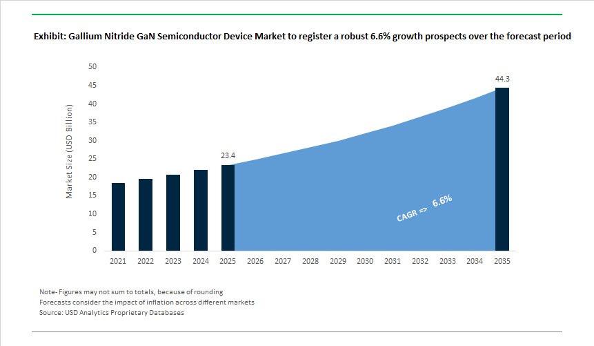
The GaN semiconductor device market (USD 23.4 billion in 2025; 6.6% CAGR to USD 44.3 billion by 2035) is expanding because GaN directly addresses a set of non-negotiable system-level constraints now facing OEMs across fast chargers, hyperscale data-centre power architectures, EV on-board and off-board charging, and RF front-ends for 5G and emerging 6G infrastructure. In these applications, incremental efficiency gains are no longer sufficient; OEMs require step-changes in power density, switching frequency, and thermal performance to reduce converter size, lower passive component count, and simplify cooling architectures at scale. GaN enables these outcomes in voltage and power ranges where silicon has reached physical limits and where SiC remains cost- or performance-inefficient.
The demand shift is both technical and commercial. At the device level, GaN’s wide bandgap and high critical electric field enable substantially lower switching losses and MHz-class operation relative to silicon MOSFETs, translating into 2-4× converter-level power-density improvements in high-volume charger and data-centre power stages. At the system level, these gains convert directly into smaller magnetics, fewer components, higher rack-level efficiency, and faster OEM design cycles - benefits that increasingly outweigh GaN’s higher device cost. In parallel, RF GaN has become the preferred power-amplifier technology for high-power C-band and millimetre-wave radios, where superior power-added efficiency, linearity, and output power per device are critical for modern base-station architectures.
Over the forecast period, market leadership will be determined less by raw device performance and more by execution at scale. Automotive-grade reliability (AEC-Q qualification, long-term thermal cycling), manufacturing maturity (wafer yields, defect density, and GaN-on-Si versus GaN-on-SiC process control), and credible cost-down roadmaps will define which suppliers transition from design wins to sustained volume shipments. Vendors able to demonstrate robust reliability data, validated MHz-switching reference designs, and secure supply-chain capacity are best positioned to capture disproportionate share as GaN adoption moves from selective substitution toward platform-level standardization in power conversion and RF modules.
The last 18 months show an intensifying shift from discrete device introductions to application-focused GaN platforms and localisation efforts. In Dec 2025, Navitas’ partnership with Cyient signalled targeted localisation and module co-development for AI datacentres and EV mobility in India, underlining OEM demand for nearby supply and faster time-to-production. In Nov 2025, Onsemi’s commercial launch of vertical GaN (vGaN) introduced an architecture intended to improve ruggedness and power density for AI computing and high-power EV applications, while Nov 2025 also saw Infineon roll out 100 V automotive-qualified GaN transistors (CoolGaN™ G1), directly addressing growing 48 V vehicle architectures.
Material and manufacturing innovation continued in Oct 2025 when Tosoh announced mass production of GaN sputtering targets - a lower-cost alternative to CVD feedstock - pointing to raw-material cost reduction strategies. Strategic consolidation and capability expansion were also important: Jun 2025 marked Renesas’ completion of its Transphorm acquisition, integrating proven 650-900 V GaN platforms to broaden high-voltage offerings. Across early 2025, Cambridge GaN Devices’ funding (Mar 2025) and Infineon’s partnerships for resonant wireless power (Jan 2025) highlighted investor and OEM confidence in GaN for high-frequency and high-efficiency power architectures.
The GaN semiconductor device market is undergoing a decisive structural shift toward vertically integrated, onshored GaN-on-Si manufacturing, driven by national security priorities, defense electronics demand, and the need to derisk wide-bandgap supply chains. Unlike silicon, GaN capacity cannot be ramped opportunistically; epitaxy, device design, and advanced packaging must be tightly coordinated to achieve yield stability at scale. As a result, governments are no longer funding isolated fabs but end-to-end GaN value chains.
In the U.S., CHIPS Act allocations through mid-2025 have prioritized power and photonic semiconductors essential for AI infrastructure, radar, and energy systems. Strategic awards to firms such as Wolfspeed and Infinera are explicitly tied to domestic epitaxy and device-scale manufacturing rather than backend-only expansion. In parallel, Europe has moved beyond pilot fabs: the EU Chips Act’s Integrated Production Facility (IPF) designation, granted in October 2025 to Infineon Technologies and STMicroelectronics, fast-tracks permitting for vertically integrated GaN lines covering epitaxy, front-end processing, and power module assembly.
The most disruptive milestone is the transition of GaN-on-Si to 300mm wafers, announced by Infineon in September 2025. By leveraging mature 300mm silicon toolsets, this shift materially reduces cost per ampere and positions GaN to reach functional cost parity with silicon MOSFETs in high-volume power applications. For OEMs, this removes the last structural barrier to GaN adoption beyond niche or premium segments.
GaN’s evolution from a 650V consumer technology into the 1.2kV+ voltage class marks a critical inflection point. Automotive and industrial power designers are now evaluating GaN not as a silicon replacement, but as a system-level alternative to SiC, particularly in 800V EV traction inverters, on-board chargers, and high-speed motor drives.
In April 2025, Fraunhofer IAF demonstrated a monolithic 1200V bidirectional GaN switch using GaN-on-insulator architectures. By integrating free-wheeling functionality on-chip, this approach significantly reduces inverter part count and switching losses—an architectural advantage over discrete SiC solutions. Reliability data emerging in late 2025 further strengthened the case: Power Integrations reported >98% efficiency from its 1250V PowiGaN HEMTs while maintaining Zero Voltage Switching at frequencies where SiC devices incur escalating losses.
Automotive qualification is accelerating accordingly. In Q1 2025, Navitas Semiconductor and Cambridge GaN Devices validated multi-level 800V inverter platforms showing up to 40% volume reduction versus silicon IGBT designs. GaN’s zero reverse-recovery behavior is emerging as the decisive advantage, enabling higher switching frequencies, smaller passive components, and lighter inverter assemblies—directly translating into vehicle range extension and packaging flexibility.
One of the most immediate commercial opportunities for GaN devices lies in AI data center power delivery, where rack power densities have surged beyond the limits of 48V architectures. Hyperscale operators are now transitioning to 800V High-Voltage DC (HVDC) distribution to support 50–100kW AI racks while constraining copper mass and thermal losses.
In May 2025, NVIDIA and Navitas Semiconductor disclosed collaboration on next-generation 800V HVDC power platforms using GaNFast ICs. These designs achieve up to 3× higher power density than silicon-based solutions, allowing GPU clusters to scale without proportionally expanding data hall footprints. Complementing this, Murata Power Solutions integrated GaN HEMTs into 5.5kW AI server power units meeting 80+ Titanium efficiency thresholds—now a baseline requirement as operators seek to curb cooling-related energy overhead.
From a systems perspective, the Open Compute Project (OCP) has highlighted GaN’s ability to operate in the MHz regime as a structural enabler: higher switching frequency reduces magnetic component volume by up to 60%, unlocking compact, high-current power stages essential for next-generation AI accelerators. This positions GaN not merely as an efficiency play, but as a foundational technology for AI infrastructure scaling.
The final high-impact opportunity is in GaN RF and MMIC devices supporting Low Earth Orbit (LEO) satellite constellations and emerging 6G networks. Explosive growth in satellite broadband traffic is driving demand for high-linearity, high-power GaN amplifiers capable of operating at Ka- and V-band frequencies under strict power budgets.
By October 2025, SpaceX had launched more than 2,500 satellites in 2025 alone, with Starlink traffic more than doubling year-on-year. This expansion directly fuels demand for GaN MMICs in both satellite payloads and cost-sensitive user terminals. In September 2025, Filtronic introduced Cerus V-band GaN SSPAs delivering up to 50 dBm (100 W) in the 47–52 GHz range—power levels essential for high-throughput, low-latency links in 6G-ready architectures.
Beyond performance, radiation tolerance is emerging as a decisive differentiator. GaN’s intrinsic resistance to displacement damage has been validated in 2025 trials, positioning it as the preferred semiconductor for 5–10 year LEO missions and next-generation >60 Tbps satellite downlinks. As constellations scale and orbit lifetimes extend, rad-hard-by-physics GaN devices are becoming core infrastructure elements rather than niche aerospace components.
GaN power discrete devices and power ICs collectively command approximately 55% of the global Gallium Nitride Semiconductor Device Market, reflecting their role as the primary value-creation layer in next-generation power electronics. This segment’s dominance is driven by GaN’s ability to switch orders of magnitude faster than silicon, enabling dramatic reductions in passive component size and unlocking unprecedented power density at the system level. The market has decisively shifted from standalone transistors toward highly integrated GaN power ICs, which combine power switching, gate driving, and protection functions on a single chip—simplifying design complexity while improving reliability. A critical inflection point reinforcing market share is the successful transition to 300mm GaN-on-silicon wafer manufacturing, which has materially improved cost economics and accelerated GaN’s penetration into high-volume applications previously dominated by silicon MOSFETs. Superior figures of merit allow equivalent or higher power output from substantially smaller die sizes, aligning directly with OEM priorities around miniaturization, thermal efficiency, and material reduction. Further, large-scale commercial shipments have validated GaN power devices as a mature, production-ready technology rather than a niche alternative. Together, these manufacturing, performance, and integration advantages position GaN power discretes and ICs as the core revenue engine of the GaN semiconductor market.
Consumer electronics and fast-charging applications account for approximately 35% of total demand in the GaN Semiconductor Device Market, making this segment the primary volume driver and the fastest pathway to mass adoption. This leadership is rooted in a structural shift in consumer expectations toward smaller, lighter, and significantly faster charging solutions across smartphones, laptops, tablets, and multi-device ecosystems. GaN technology enables step-change improvements in power density and efficiency, allowing high-wattage chargers to be produced in form factors once reserved for low-power adapters, without compromising thermal safety. Market share is further reinforced by efficiency gains that materially reduce heat generation, eliminating the need for bulky heatsinks and enabling minimalist industrial design—an increasingly important differentiator in consumer hardware. The segment has reached a critical adoption threshold, with double-digit penetration in mobile charging signaling the onset of an S-curve expansion phase. Universal engagement from top-tier consumer electronics OEMs further validates GaN as the new default architecture for fast charging platforms. As charging speed, portability, and energy efficiency become baseline expectations rather than premium features, consumer electronics remains the central demand anchor sustaining GaN’s market leadership.
 Semiconductor Device Market Share by Application, 2025.png)
The GaN vendor ecosystem is split between vertically integrated incumbents pushing wafer-scale cost reductions and pure-play innovators optimising device architectures and IC integration. Competitive advantage flows from process scale (300 mm GaN-on-Si), packaging and Si-driver integration, proven reliability metrics (short-circuit withstand, thermal cycling), and strong application reference designs.
Infineon combines strategic M&A and process scale to lead mainstream adoption: after acquiring GaN Systems, Infineon has advanced GaN-on-Si production on 300 mm wafers to lower cost-per-unit and increase throughput. Its CoolGaN™ portfolio includes automotive-qualified 100 V devices and integrated e-mode ICs with drivers, targeting 48 V automotive systems and high-efficiency PFC/DC-DC stages in data-centre PSUs. Infineon’s strength is marrying GaN device IP with established silicon-based manufacturing and broad power-IC portfolios for system integrators.
Navitas focuses on highly integrated GaNFast™ power ICs that combine GaN power FETs with drivers and protection circuitry to simplify board-level design and EMI control. Dominant in high-performance chargers and adapters, Navitas is expanding into higher-power applications and has pursued regional partnerships (e.g., Cyient) to localize module development for growing AI and EV markets. Its integration-first model reduces BOM and accelerates customer qualification cycles.
EPC is the pioneer for enhancement-mode GaN HEMTs in low-voltage, high-speed domains (15-350 V). It leads in Lidar and DC/DC conversion where ultra-fast switching delivers superior pulse performance and high power density - EPC’s ePower™ ICs combine paired GaN FETs and gate drivers to minimize parasitics and enable compact half-bridge designs that reach multiple kW/in³ in power density.
By integrating Transphorm, Renesas strengthened its high-voltage GaN portfolio (650-900 V) and robustness credentials (patented short-circuit withstand times). Renesas’ strategy couples GaN switches with its MCU expertise, enabling SiP solutions and complete power modules tailored for industrial, EV traction and renewable-energy inverters, where voltage ruggedness and certified reliability are essential.
ST leverages its process capabilities (including 300 mm ambitions) and broad power-IC catalogue to deliver integrated MasterGaN half-bridge modules (GaN FET + gate driver). ST’s approach is system-oriented - combining MCU, power stage and reference designs - which accelerates adoption in motor control, on-board EV chargers and industrial converters by offering validated, compact power subsystems.
The United States has positioned gallium nitride as a national security semiconductor, integrating GaN devices into defense electronics, AI data centers, and high-voltage power conversion. In 2025, the U.S. Department of Commerce finalized a $285 million CHIPS and Science Act award to establish a Digital Twin manufacturing institute in North Carolina, focused on yield optimization and defect reduction for compound semiconductors. This initiative directly strengthens RF GaN supply for radar, electronic warfare, and satellite communications while accelerating power GaN adoption in hyperscale data centers.
On the industrial side, Wolfspeed continues scaling its John Palmour Manufacturing Center, reinforcing domestic GaN wafer and device capacity. Complementing supply-side support, tariff escalation effective January 2025 imposed a 50% duty on select semiconductor imports, insulating U.S. GaN fabs from global price compression and reinforcing reshoring momentum across defense-grade and power electronics segments.
China remains the world’s most influential actor in the GaN ecosystem due to its dominance in raw gallium refining. Following tightened Western controls, the Ministry of Commerce of the People's Republic of China enforced a total export ban on gallium and germanium to the United States, triggering a sharp price spike in global markets by mid-2025. This move has transformed gallium into a strategic leverage material rather than a commodity input.
Domestically, China is simultaneously scaling device manufacturing. The National Integrated Circuit Industry Investment Fund (Big Fund III) deployed significant capital toward Innoscience, operator of the world’s largest 200 mm GaN-on-Si capacity. Integration into EV platforms is accelerating, with state OEMs embedding GaN power modules to improve inverter efficiency and reduce system losses.
Japan’s GaN strategy is tightly coupled with its automotive supply chain, prioritizing reliability, longevity, and thermal efficiency. In 2025, DENSO and ROHM formalized a strategic partnership securing GaN power devices for next-generation EV inverters, anchoring GaN deeply into Japan’s mobility roadmap.
Material science leadership remains a differentiator. Japanese suppliers reported 300 mm GaN-on-Si process milestones, a critical step toward cost parity with silicon. Backed by the Ministry of Economy, Trade and Industry, Japan continues subsidizing the conversion of legacy fabs into compound semiconductor lines, reinforcing long-term supply security for automotive and industrial power electronics.
Europe’s GaN push is framed around strategic autonomy and energy efficiency, coordinated under the European Chips Act. In March 2025, nine EU member states-led by Germany and France-launched a semiconductor coalition targeting €200 billion in cumulative investment by 2035, explicitly covering industrial and automotive GaN.
A European IDM demonstrated a 300 mm GaN-on-Si production line, delivering a step-change in die economics versus 200 mm processes. Simultaneously, EU Green Deal directives are favoring GaN-based power supplies in data centers and industrial drives, where 10–25% efficiency gains materially reduce lifecycle emissions-cementing GaN’s role in Europe’s decarbonization agenda.
Taiwan’s GaN trajectory is defined by a strategic realignment toward AI. In a pivotal 2025 announcement, TSMC confirmed its exit from GaN foundry services by 2027, repurposing capacity toward advanced packaging (CoWoS) for AI accelerators. This decision reflects higher returns and strategic priority in heterogeneous integration.
The exit has created opportunity for PSMC, which signed new partnerships in 2025 to absorb global GaN wafer demand. Taiwan thus remains relevant in GaN, albeit through specialized foundry roles rather than broad ecosystem leadership.
India is transitioning from design-centric participation to active GaN fabrication, positioning itself as a trusted, geopolitically neutral supply partner. At Semicon India 2025, the India Semiconductor Mission formalized agreements with Tata Electronics to accelerate a compound semiconductor fab in Gujarat, targeting GaN for 5G infrastructure and defense electronics.
Policy support is decisive. Under the Modified Semicon India Programme, the government offers 50% capital expenditure support for compound semiconductor fabs, while a ₹4,500 crore modernization of the SCL Mohali facility is transforming it into a national GaN R&D hub-laying the foundation for long-term ecosystem depth.
|
Country |
Primary Strategic Driver |
2025 Key Policy / Event |
Focus Technology |
|
United States |
National Security & Data Centers |
CHIPS Act $285M Digital Twin Institute |
RF GaN & Power GaN |
|
China |
Resource Monopoly |
Gallium Export Ban |
200 mm GaN-on-Si |
|
Japan |
Automotive Intelligence |
DENSO–ROHM Partnership |
EV Inverters & Analog ICs |
|
European Union |
Strategic Autonomy |
Semiconductor Coalition |
300 mm Industrial GaN |
|
Taiwan |
AI Dominance |
TSMC GaN Exit |
Advanced Packaging |
|
India |
Supply Chain Trust |
₹4,500 Cr SCL Modernization |
5G & Defense GaN |
|
Parameter |
Details |
|
Market Size (2025) |
$23.4 Billion |
|
Market Size (2035) |
$44.3 Billion |
|
Market Growth Rate |
6.6% |
|
Segments |
By Device Type (GaN Power Discrete Devices, GaN RF Devices, GaN Integrated Circuits, GaN Optoelectronic Devices), By Substrate Technology (GaN-on-Silicon, GaN-on-Silicon Carbide, GaN-on-Sapphire, GaN-on-GaN, GaN-on-Diamond), By Application (Consumer Electronics, Telecommunications, Automotive & Mobility, Data Centers & AI, Industrial & Energy, Aerospace & Defense) |
|
Study Period |
2019- 2024 and 2025-2034 |
|
Units |
Revenue (USD) |
|
Qualitative Analysis |
Porter’s Five Forces, SWOT Profile, Market Share, Scenario Forecasts, Market Ecosystem, Company Ranking, Market Dynamics, Industry Benchmarking |
|
Companies |
Infineon Technologies AG, Wolfspeed Inc., onsemi, STMicroelectronics, Navitas Semiconductor, Innoscience, EPC (Efficient Power Conversion), NXP Semiconductors N.V., Qorvo Inc., Sumitomo Electric Device Innovations, Texas Instruments Incorporated, MACOM Technology Solutions, Panasonic Corporation, Renesas Electronics Corporation, GaN Systems / Transphorm Inc. |
|
Countries |
US, Canada, Mexico, Germany, France, Spain, Italy, UK, Russia, China, India, Japan, South Korea, Australia, South East Asia, Brazil, Argentina, Middle East, Africa |
*- List not Exhaustive
Table of Contents: Gallium Nitride (GaN) Semiconductor Device Market
1. Executive Summary
1.1. Market Highlights
1.2. Key Findings
1.3. Global Market Snapshot
2. Gallium Nitride (GaN) Semiconductor Device Market Landscape & Outlook (2025–2034)
2.1. Introduction to GaN Semiconductor Device Market
2.2. Market Valuation and Growth Projections (2025–2034)
2.3. Power Density, MHz Switching, and System-Level Efficiency Drivers
2.4. Manufacturing Maturity, Yield Economics, and Cost-Down Roadmaps
2.5. Reliability Standards, Automotive Qualification, and Supply-Chain Localization
3. Innovations Reshaping the GaN Semiconductor Device Market
3.1. Trend: Vertical GaN (vGaN) and 300 mm GaN-on-Silicon Scaling
3.2. Trend: 800 V HVDC Architectures for AI Data Centers and EV Platforms
3.3. Opportunity: 1.2 kV–Class GaN for Automotive and Industrial Power Conversion
3.4. Opportunity: GaN MMICs for LEO Satcom, 6G, and Space-Grade RF Systems
4. Competitive Landscape and Strategic Initiatives
4.1. Mergers, Acquisitions, and Ecosystem Consolidation
4.2. R&D in Device Architecture, Packaging, and Wafer-Scale Manufacturing
4.3. Sustainability, Energy Efficiency, and ESG Alignment
4.4. Market Expansion, Onshoring, and Regional Capacity Build-Out
5. Market Share and Segmentation Insights: Gallium Nitride (GaN) Semiconductor Device Market
5.1. By Device Type
5.1.1. GaN Power Discrete Devices
5.1.2. GaN Radio Frequency (RF) Devices
5.1.3. GaN Integrated Circuits
5.1.4. GaN Optoelectronic Devices
5.2. By Substrate Technology
5.2.1. GaN-on-Silicon
5.2.2. GaN-on-Silicon Carbide
5.2.3. GaN-on-Sapphire
5.2.4. GaN-on-GaN
5.2.5. GaN-on-Diamond
5.3. By Application
5.3.1. Consumer Electronics
5.3.2. Telecommunications
5.3.3. Automotive and Mobility
5.3.4. Data Centers and Artificial Intelligence
5.3.5. Industrial and Energy
5.3.6. Aerospace and Defense
6. Country Analysis and Outlook of GaN Semiconductor Device Market
6.1. United States
6.2. Canada
6.3. Mexico
6.4. Germany
6.5. France
6.6. Spain
6.7. Italy
6.8. United Kingdom
6.9. Russia
6.10. China
6.11. India
6.12. Japan
6.13. South Korea
6.14. Australia
6.15. South East Asia
6.16. Brazil
6.17. Argentina
6.18. Middle East
6.19. Africa
7. GaN Semiconductor Device Market Size Outlook by Region (2025–2034)
7.1. North America GaN Semiconductor Device Market Size Outlook to 2034
7.1.1. By Device Type
7.1.2. By Substrate Technology
7.1.3. By Application
7.1.4. By Country
7.2. Europe GaN Semiconductor Device Market Size Outlook to 2034
7.2.1. By Device Type
7.2.2. By Substrate Technology
7.2.3. By Application
7.2.4. By Country
7.3. Asia Pacific GaN Semiconductor Device Market Size Outlook to 2034
7.3.1. By Device Type
7.3.2. By Substrate Technology
7.3.3. By Application
7.3.4. By Country
7.4. South America GaN Semiconductor Device Market Size Outlook to 2034
7.4.1. By Device Type
7.4.2. By Substrate Technology
7.4.3. By Application
7.4.4. By Country
7.5. Middle East and Africa GaN Semiconductor Device Market Size Outlook to 2034
7.5.1. By Device Type
7.5.2. By Substrate Technology
7.5.3. By Application
7.5.4. By Country
8. Company Profiles: Leading Players in the Gallium Nitride (GaN) Semiconductor Device Market
8.1. Infineon Technologies AG
8.2. Wolfspeed, Inc.
8.3. onsemi
8.4. STMicroelectronics
8.5. Navitas Semiconductor
8.6. Innoscience
8.7. EPC (Efficient Power Conversion)
8.8. NXP Semiconductors N.V.
8.9. Qorvo, Inc.
8.10. Sumitomo Electric Device Innovations
8.11. Texas Instruments Incorporated
8.12. MACOM Technology Solutions
8.13. Panasonic Corporation
8.14. Renesas Electronics Corporation
8.15. GaN Systems / Transphorm Inc.
9. Methodology
9.1. Research Scope
9.2. Market Research Approach
9.3. Market Sizing and Forecasting Model
9.4. Research Coverage
9.5. Data Horizon
9.6. Deliverables
10. Appendix
10.1. Acronyms and Abbreviations
10.2. List of Tables
10.3. List of Figures
The global GaN Semiconductor Device Market was valued at USD 23.4 billion in 2025 and is forecast to reach USD 44.3 billion by 2035, expanding at a CAGR of 6.6% during 2026–2035. Growth is anchored in fast charging, AI data-center power, EV electrification, and RF infrastructure.
GaN enables MHz-class switching, lower switching losses, and significantly higher power density than silicon MOSFETs. These advantages reduce passive component size, simplify cooling, and shrink converter footprints, delivering system-level efficiency and cost benefits that outweigh higher device prices.
GaN power discrete devices and integrated power ICs account for roughly 55% of total market revenue. Their dominance is driven by adoption in fast chargers, data-center PSUs, EV on-board chargers, and high-density DC-DC converters where integration, reliability, and power density are critical.
AI data centers are transitioning to 800V HVDC architectures to support 50–100 kW racks, creating strong demand for GaN devices that operate efficiently at high frequency and voltage. GaN enables up to 3× higher power density and major reductions in copper and magnetic component size.
Leading players include Infineon Technologies, Wolfspeed, onsemi, STMicroelectronics, Navitas Semiconductor, Innoscience, EPC, Qorvo, Renesas Electronics, NXP Semiconductors, MACOM, and Sumitomo Electric. Leaders differentiate through 300 mm GaN-on-Si scaling, automotive qualification, and system-level integration.