Monocrystalline Silicon Market Overview: N-Type Solar Wafers, Advanced Logic Nodes, and Strategic Substrate Demand Drive Growth
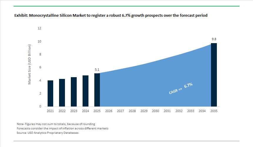
The Monocrystalline Silicon Market, valued at USD 5.1 billion in 2025, is projected to reach USD 9.8 billion by 2035 at a 6.7% CAGR, propelled by rapid advancements in photovoltaic grade N-type wafers and persistent demand for ultra-high-purity semiconductor silicon used in advanced logic, memory, and power electronics. Solar manufacturers such as LONGi, Jinko, and JA Solar are accelerating the transition from P-type PERC to N-type TOPCon and HJT architectures, with commercial cell efficiencies now surpassing 25%, requiring high-lifetime, low-oxygen monocrystalline silicon. At the same time, wafer producers are scaling G12 and M10 formats to improve throughput and reduce LCOE, pushing crystal growers to optimize ingot diameter stability, resistivity uniformity, and thermal field control for large-format pulling.
On the semiconductor side, leading fabs demand sub-ppbw metal impurity levels, defect densities suitable for 5 nm and below, and high-resistivity float-zone (FZ) wafers for specialty power devices, RF filters, and high-voltage components. Manufacturers such as SUMCO, Shin-Etsu, and Siltronic continue to refine Czochralski (CZ), magnetic-CZ (MCZ), continuous-CZ, and FZ techniques. The industry is also investing in kerf-loss recycling technologies-through companies like Norwegian Crystals, REC Silicon, and PV circularity initiatives-which can recover >90% of wire-sawing material losses, lowering polysilicon dependency and stabilizing wafer economics. The market’s growth is further reinforced by national supply-chain initiatives in the U.S., Europe, Japan, and South Korea, where monocrystalline silicon is increasingly viewed as a strategic substrate for power semiconductors, defense electronics, solar manufacturing sovereignty, and wafer-to-module integration.
Monocrystalline Silicon Market Analysis: Capacity Expansion, Purity Breakthroughs, and Large-Diameter Wafer Scaling
The market is witnessing parallel advances in wafer efficiency records, capacity ramp-ups for N-type wafers, and R&D towards defect-free, large-diameter crystals. In January 2025 a leading solar OEM publicly confirmed that ~80% of its planned yearly capacity would be based on N-Type TOPCon cells - a clear production signal that wafer customers are prioritizing N-type mono feedstock. February 2025 saw LONGi announce a multi-billion dollar investment in a fully integrated monocrystalline silicon-to-module production base in Vietnam, illustrating how manufacturers are vertically integrating to secure polysilicon-to-module throughput and localize production capacity.
Through mid-2025 and into late 2025 the focus broadened to purity and large-wafer precision. In May 2025 a semiconductor wafer supplier launched argon-annealed 300 mm polished wafers targeting sub-5 nm logic, improving surface quality and lowering defect density for advanced nodes. September 2025 highlighted strategic supply resilience when the US Department of Defense awarded a contract to secure domestic high-purity Si and SiC substrates, reinforcing government support for onshore critical material fabrication. Research milestones continued: October 2025 academic/industry teams published methods to produce 300 mm Floating Zone (FZ) monocrystalline silicon with an exceptionally high defect-free rate, and in November 2025 wafer manufacturers in China announced successful ramp-up of Phase III N-type wafer capacity (adding up to 30 GW equivalent), strengthening global solar wafer availability. The period closed with a technology milestone in December 2025, when LONGi announced a world-record 34.85% efficiency for a perovskite-silicon tandem cell - an innovation that will ultimately pressure wafer suppliers to support tandem architectures and higher crystalline quality requirements.
Monocrystalline Silicon Market: Trends and Opportunities
Accelerated Transition to Larger, Thinner N-Type Wafers Reshaping the PV Value Chain
The monocrystalline silicon market has entered a structurally different phase as the photovoltaic industry decisively exits the PERC era and standardizes around N-type architectures, particularly TOPCon and HJT. This transition is not incremental; it is redefining ingot purity, wafer geometry, and thickness economics simultaneously. According to the 16th edition of the International Technology Roadmap for Photovoltaic, N-type wafers crossed a critical inflection in April 2025, accounting for roughly 70% of global adoption for the first time. This shift has accelerated the move toward rectangular M10 and G12 wafer formats, enabling module power classes to approach and exceed 700 W while reducing balance-of-system costs.
Wafer thinning has emerged as the most powerful lever for cost and efficiency optimization. By late 2025, TOPCon mass production stabilized around 130–140 μm, while HJT leaders pushed aggressively toward 110–120 μm, materially improving kerf-loss efficiency and wafer yield per kilogram of monocrystalline ingot. These thinner wafers place new demands on crystal quality—oxygen levels below 12 ppma and bulk lifetimes above 2 ms are now baseline requirements rather than premium specifications. Despite inventory volatility, production discipline remains strong. Data released in October 2025 by OPIS indicates global wafer output exceeding 60 GW per month, with utilization rates above 60% as manufacturers rapidly retrofit legacy P-type lines to N-type TOPCon. Strategically, N-type monocrystalline substrates are also being positioned as tandem-ready platforms, with laboratory TOPCon efficiencies reaching 26.1%, reinforcing silicon’s relevance even as the industry approaches the single-junction theoretical ceiling.
Strategic Onshoring of High-Purity Polysilicon and Ingot Capacity
Energy security and industrial policy are now directly shaping the monocrystalline silicon supply chain, driving a shift from global optimization toward regional self-sufficiency. In the United States, final regulations under the CHIPS Act and related clean-energy provisions introduced a 25% Investment Tax Credit for solar ingot and wafer manufacturing—an unprecedented move for a country that historically lacked any commercial ingot-to-wafer base. By March 2025, domestic announcements totaled roughly 13 GW of ingot and 24 GW of wafer capacity, signaling a deliberate attempt to rebuild upstream monocrystalline capability rather than remain dependent on imports.
India is pursuing an even more vertically integrated model. Under the Production Linked Incentive framework administered by the Ministry of New and Renewable Energy, a fully integrated 20 GW solar giga-factory led by Reliance Industries is scheduled for commissioning by FY 2025–26, spanning polysilicon through cells. Recognizing upstream bottlenecks, the Indian government issued financing directives in December 2025 to institutions such as IREDA to prioritize polysilicon and ingot-wafer investments. While cost disparities remain—U.S. polysilicon production can be up to five times more expensive than Chinese output—production credits under Section 45X of the Inflation Reduction Act are narrowing the gap, transforming monocrystalline silicon from a purely cost-driven commodity into a geopolitically strategic material.
High-Resistivity Silicon Unlocks Power Electronics and Grid-Scale Electrification
Beyond photovoltaics, monocrystalline silicon is seeing a high-margin expansion into power semiconductor substrates, driven by electrification across EVs, renewables, and smart grids. Insulated-Gate Bipolar Transistors (IGBTs) require high-resistivity CZ and Float-Zone silicon—typically 100–1,000 Ω·cm—to manage high voltages with minimal leakage and thermal loss. Demand is being reinforced by a clear manufacturing transition: leading device makers are shifting IGBT production from 200 mm to 300 mm wafers to improve die economics and throughput. Companies such as Infineon and onsemi are adopting Neutron Transmutation Doping (NTD) to achieve ultra-uniform resistivity for 1,700 V and above applications—an area where monocrystalline quality directly determines device yield.
System-level electrification is amplifying this pull. The International Energy Agency reported that one in five cars sold globally in 2024 was electric, and by 2025 the proliferation of DC fast-charging infrastructure has increased demand for high-speed IGBTs with minimal defect tolerance. In parallel, policy-driven semiconductor localization is reinforcing domestic substrate demand. In December 2025, approvals under the Semicon India Programme covered ten units with investments of ₹1.6 lakh crore, including silicon fabs and advanced packaging facilities focused on industrial and power electronics—creating a durable opportunity for monocrystalline silicon producers beyond the solar cycle.
Ultra-High-Purity Silicon Emerges as a Critical Input for Quantum Computing
Quantum computing is opening a fundamentally new demand frontier for monocrystalline silicon—one defined not by volume, but by atomic-level purity. Conventional silicon contains the isotope ²⁹Si, whose nuclear spin disrupts qubit coherence and renders it unsuitable for scalable quantum processors. As a result, isotopically enriched Silicon-28 (²⁸Si) is becoming a strategic material for next-generation computing architectures. In 2025, the market for ²⁸Si moved decisively from academic supply to early industrialization, with quantum computing projected to consume the majority of output by the end of the decade.
A key inflection came from research published by teams at the University of Melbourne and the University of Manchester, demonstrating a scalable purification technique that reduced ²⁹Si concentration from 4.5% to two parts per million. Crucially, the process relies on standard ion implanters already installed in most semiconductor fabs, dramatically lowering barriers for monocrystalline silicon producers to enter the quantum substrate market. This has direct implications for coherence performance: ultra-pure ²⁸Si substrates are enabling orders-of-magnitude improvements in qubit coherence times, a prerequisite for error-corrected quantum computing. With more than $10 billion in global public and private quantum programs active by late 2025, ultra-high-purity monocrystalline silicon is transitioning from a laboratory curiosity into a strategically scarce, high-value material class.
Monocrystalline Silicon Market Share Analysis
Market Share by Application: Photovoltaics Cement Monocrystalline Silicon as the Solar Industry’s Core Material
Photovoltaics account for approximately 85% of total demand in the global Monocrystalline Silicon Market, firmly establishing solar energy as the dominant application driving volume, investment, and technology evolution. This overwhelming share is a direct result of monocrystalline silicon’s single-crystal structure, which enables superior electron mobility and delivers the highest commercially viable energy conversion efficiencies in mass-produced solar modules. In 2025, leading manufacturers have pushed commercial module efficiencies beyond the 25% threshold, allowing substantially higher power output from the same rooftop or land footprint—a decisive advantage in space-constrained urban markets and land-intensive utility-scale projects alike. Market dominance is further reinforced by the industry-wide shift toward N-type monocrystalline silicon, which eliminates light-induced degradation and preserves output stability over the full operating life of the panel. Temperature resilience has also become a critical driver, as monocrystalline cells now exhibit industry-leading temperature coefficients, making them the preferred choice for high-irradiance, high-heat regions where performance losses directly impact project economics. The rise of bifacial monocrystalline modules, capable of harvesting reflected light from both sides, further amplifies energy yield without increasing material usage, strengthening return-on-investment metrics for developers. Together, these efficiency, durability, and yield advantages position photovoltaics as the structural engine of monocrystalline silicon demand and explain its commanding share of the global market.
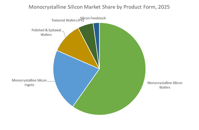
Market Share by Product Form: Monocrystalline Wafers Dominate Through Scale and Yield Economics
Monocrystalline silicon wafers represent approximately 55% of market demand, reflecting their central role as the foundational input for both solar cells and advanced semiconductor devices. This segment’s leadership is anchored in the industry’s relentless focus on scale, yield optimization, and material efficiency, where wafer dimensions and quality directly influence unit economics. In semiconductor manufacturing, the widespread adoption of 300mm wafers has significantly increased chip output per wafer, lowering cost per die and enabling the economic production of high-performance processors and memory devices. In parallel, solar manufacturers are pushing toward ultra-thin monocrystalline wafers, reducing silicon consumption while maintaining high conversion efficiency—an innovation that directly improves margins and supports emerging form factors such as lightweight and flexible modules. Advanced surface texturing techniques further enhance wafer value by minimizing optical losses and maximizing photon absorption, ensuring that each wafer delivers higher electrical output per unit area. At the high-purity end, monocrystalline wafers remain indispensable for cutting-edge semiconductor nodes, where ultra-high purity silicon is required to prevent electrical leakage and thermal instability. These combined scale, efficiency, and purity advantages explain why monocrystalline wafers remain the commercial and technological backbone of the global monocrystalline silicon market.
Competitive Landscape: Wafer Specialists, Polysilicon Leaders, and Vertically Integrated Scale Players
The competitive structure blends vertically integrated solar leaders, hyper-pure polysilicon producers, and wafer specialists focused on 300 mm semiconductor substrates. Competitive differentiation is driven by RCz/MCZ/FZ crystal-growth excellence, diamond-wire slicing efficiency, ultra-clean polishing/anneal processes, wafer size roadmaps (G12/M10/300 mm), and strategic localization of production to meet OEM and defense sourcing requirements. Buyers evaluate suppliers on throughput, defect rates, traceable purity specs, and the ability to supply both PV and IC markets without cross-contamination risks.
Longi Green Energy - Large-Scale Mono Production and Vertical Integration Into Module Readiness
LONGi is a global leader in monocrystalline silicon manufacturing with proprietary RCZ crystal-growth and diamond-wire slicing technologies that drive large-scale cost efficiencies for PV wafers. The company’s multi-billion dollar Vietnam investment (announced Feb 2025) and ongoing R&D toward tandem cell compatibility position LONGi to supply both high-volume G12/M10 wafer formats and future tandem-ready substrates. LONGi’s record 34.85% tandem cell achievement (announced Dec 2025) underscores its strategy to align wafer specs with next-generation perovskite-silicon module needs.
Wacker Chemie AG - Hyperpure Polysilicon and Purity Solutions For Semiconductor and PV Feedstocks
Wacker is renowned for hyperpure polysilicon production-material that underpins both IC-grade and high-efficiency PV monocrystals. With major sites in Germany and the US, Wacker’s investments (including a new cleaning line in Burghausen in 2025) strengthen its ability to supply ultra-low impurity feedstock and tailored polysilicon grades for demanding microelectronics and TOPCon/HJT wafer fabrication. Wacker’s R&D partnerships on kerf recovery and silicon recycling aim to improve feedstock circularity and reduce raw-material costs for wafer makers.
SUMCO Corporation - 300 Mm Wafer Mastery For Advanced Logic and Memory Device Fabs
SUMCO is a top global provider of large-diameter monocrystalline silicon wafers, especially 300 mm substrates required by advanced logic and memory fabs. The company’s strength lies in precise CZ/FZ crystal growth, epitaxial and SOI wafer formats, and polishing processes that deliver ultra-flat, defect-free surfaces for sub-5 nm nodes. SUMCO’s vertical integration of crystal growth through final wafer finishing enables it to meet the most stringent flatness and defect tolerance demanded by leading semiconductor manufacturers.
Zhejiang Zhonghuan Advanced Materials - Dual Strategy Across Solar High-Volume and IC-Grade Wafers
Zhejiang Zhonghuan executes a two-pronged strategy: high-volume G-family solar wafer production and selective expansion into IC-grade, 300 mm wafer capacity for power and logic markets. Its industrial footprint across multiple centers supports large monthly slice outputs (hundreds of thousands of wafers), and recent technological steps toward COP-free 300 mm ingots are aimed at reducing crystal-originated pits and boosting yield for VLSI applications. Zhonghuan’s scale economics make it a leading supplier for high-throughput PV lines while enabling targeted moves into higher-value semiconductor substrates.
China continues to anchor the global monocrystalline silicon market through unmatched vertical integration spanning polysilicon, ingots, wafers, cells, and modules. In 2024–2025, leading manufacturers such as LONGi Green Energy and Jinko Solar completed an industry-wide pivot from P-type PERC to N-type TOPCon architectures, fundamentally resetting efficiency benchmarks for monocrystalline wafers. This technological transition has been supported by aggressive capacity expansion, with China hosting close to 1,200 GW of module manufacturing capacity, increasingly powered by captive renewable energy in western provinces to lower the carbon intensity of crystal pulling. On the trade front, MOFCOM’s November 2025 suspension of select export restrictions following the Busan Accord helped stabilize global ingot and wafer pricing after extreme volatility. Despite global oversupply pressures, China’s scale, cost leadership, and process maturity continue to define global pricing dynamics in monocrystalline silicon.
United States’ IRA- and CHIPS-Backed Manufacturing Resurgence
The United States monocrystalline silicon market is being reshaped by policy-driven re-industrialization under the Inflation Reduction Act (IRA) and the CHIPS and Science Act. Federal subsidies are strategically directed toward restoring domestic ingot-to-wafer capabilities for 300 mm silicon wafers, which are critical for advanced logic and memory fabrication. While thin-film players remain active, silicon-based manufacturers benefit from protected pricing created by cumulative tariffs exceeding 100% on select imports as of late 2025. This trade insulation, combined with manufacturing tax credits and investment incentives, is creating a differentiated U.S. market focused on supply chain security rather than cost competition. The result is a structurally higher-priced but strategically resilient domestic monocrystalline silicon ecosystem aligned with national semiconductor and energy security goals.
India’s PLI 2.0 Driving Integrated Solar Silicon Ecosystems
India is executing one of the most aggressive localization strategies in the monocrystalline silicon market through its Production Linked Incentive (PLI) framework. By mid-2025, operational ingot-wafer capacity under PLI had reached 2.2 GW, marking India’s transition from module assembly toward upstream silicon processing. Tranche-II allocations awarded by SECI to major conglomerates such as Reliance Industries are enabling the build-out of fully integrated polysilicon-to-module facilities exceeding 39 GW. These investments are already translating into reduced import dependency, with solar module imports declining sharply between FY22 and FY25. India’s strategy positions monocrystalline silicon not merely as a solar input, but as a cornerstone of energy sovereignty and industrial capability under the Atmanirbhar Bharat agenda.
South Korea’s Mega Semiconductor Cluster and Wafer Demand Intensification
South Korea’s monocrystalline silicon demand is overwhelmingly semiconductor-driven, reinforced by the government’s long-term mega cluster roadmap. The planned build-out of 16 advanced fabs under a multi-decade investment program is creating sustained demand for prime-grade 300 mm monocrystalline wafers. To mitigate supply risks, Korea is localizing materials and equipment production through designated MPE complexes, reducing reliance on external silicon wafer suppliers. Generous tax deductions for investments in national strategic technologies further incentivize domestic crystal growth and wafer finishing capabilities. This policy-industrial alignment cements South Korea as a premium demand center for ultra-high-purity monocrystalline silicon.
Germany and the European Union’s Re-shoring and Carbon Regulation Push
Across Germany and the wider European Union, monocrystalline silicon policy is tightly coupled with energy security and carbon regulation. The European Solar Industry Alliance’s push to re-shore 30 GW of annual solar manufacturing capacity reflects concerns over external dependence for wafers and cells. Regulatory instruments such as the CBAM and revisions to Germany’s EEG are indirectly favoring low-carbon monocrystalline modules, particularly high-efficiency HJT and IBC technologies suited for space-constrained urban installations. While Europe remains cost-challenged relative to Asia, policy support and carbon transparency are carving out a niche for premium, low-emission monocrystalline silicon products.
Japan’s Materials DX and High-Purity Silicon Leadership
Japan maintains its strategic relevance in the monocrystalline silicon market through precision manufacturing and digitalized materials science. Government-backed Materials Research DX platforms are leveraging AI to optimize crystal growth, reduce defect density, and improve yields in large-diameter ingots. Corporate leaders such as Shin-Etsu Chemical and SUMCO are expanding 300 mm wafer capacity to meet rising demand from AI servers, cloud infrastructure, and advanced logic chips. Japan’s role is less about volume expansion and more about supplying the highest-purity monocrystalline silicon to the global semiconductor industry.
Strategic Development Matrix: Monocrystalline Silicon Market (2025)
Monocrystalline Silicon Market Development Matrix by Country
|
Country / Region
|
Primary Strategic Driver
|
Key 2025 Development
|
Core Market Focus
|
|
China
|
Vertical integration & N-type shift
|
Full TOPCon transition, export stabilization
|
Solar wafers and modules
|
|
United States
|
IRA & CHIPS reshoring
|
Subsidized 300 mm wafer manufacturing
|
Semiconductors, energy security
|
|
India
|
PLI 2.0 localization
|
Integrated polysilicon-to-module capacity
|
Solar self-reliance
|
|
South Korea
|
Mega semiconductor cluster
|
16-fab roadmap, MPE localization
|
Advanced logic & memory wafers
|
|
Germany & EU
|
Energy security & CBAM
|
ESIA re-shoring, low-carbon modules
|
High-efficiency solar
|
|
Japan
|
Materials DX leadership
|
AI-optimized crystal growth
|
Ultra-pure semiconductor wafers
|
Monocrystalline Silicon Market Report Scope
Monocrystalline Silicon Market
|
Parameter
|
Details
|
|
Market Size (2025)
|
$5.1 Billion
|
|
Market Size (2035)
|
$9.8 Billion
|
|
Market Growth Rate
|
6.7%
|
|
Segments
|
By End-User Industry (Photovoltaics, Semiconductors, Power Electronics, Others), By Product Form (Monocrystalline Silicon Ingots, Wafers, Polished Wafers, Textured Wafers, Epitaxial Wafers, Silicon Feedstock), By Crystal Growth Method (Czochralski Process, Float Zone Process, Recharge Czochralski Process, Directional Solidification Process), By Wafer Size (200 mm, 300 mm, 450 mm, M6, M10, G12), By Doping Type (P-Type, N-Type)
|
|
Study Period
|
2019- 2024 and 2025-2034
|
|
Units
|
Revenue (USD)
|
|
Qualitative Analysis
|
Porter’s Five Forces, SWOT Profile, Market Share, Scenario Forecasts, Market Ecosystem, Company Ranking, Market Dynamics, Industry Benchmarking
|
|
Companies
|
LONGi Green Energy Technology Co., Ltd., TCL Zhonghuan Renewable Energy Technology Co., Ltd., Wuxi Shangji Automation Co., Ltd., JinkoSolar Holding Co., Ltd., Trina Solar Co., Ltd., SUMCO Corporation, Shin-Etsu Chemical Co., Ltd., Siltronic AG, GlobalWafers Co., Ltd., Tongwei Co., Ltd., Daqo New Energy Corp., SK Siltron Co., Ltd., Hanwha Q Cells Co., Ltd., Ferrotec Holdings Corporation
|
|
Countries
|
US, Canada, Mexico, Germany, France, Spain, Italy, UK, Russia, China, India, Japan, South Korea, Australia, South East Asia, Brazil, Argentina, Middle East, Africa
|
Monocrystalline Silicon Market Segmentation
By End-User Industry
- Photovoltaics
- Semiconductors
- Power Electronics
- Others
By Product Form
- Monocrystalline Silicon Ingots
- Monocrystalline Silicon Wafers
- Polished Wafers
- Textured Wafers
- Epitaxial Wafers
- Silicon Feedstock
By Crystal Growth Method
- Czochralski Process
- Float Zone Process
- Recharge Czochralski Process
- Directional Solidification Process
By Wafer Size
- 200 mm
- 300 mm
- 450 mm
- M6
- M10
- G12
By Doping Type
- P-Type Monocrystalline Silicon
- N-Type Monocrystalline Silicon
By Region
- North America (United States, Canada, Mexico)
- Europe (Germany, France, United Kingdom, Spain, Italy, Rest of Europe)
- Asia Pacific (China, India, Japan, South Korea, Australia, Rest of APAC)
- South and Central America (Brazil, Argentina, Rest of SCA)
- Middle East and Africa (Saudi Arabia, UAE, South Africa, Rest of Middle East, Rest of Africa)
Top Companies in Monocrystalline Silicon Market
- LONGi Green Energy Technology Co., Ltd.
- TCL Zhonghuan Renewable Energy Technology Co., Ltd.
- Wuxi Shangji Automation Co., Ltd.
- JinkoSolar Holding Co., Ltd.
- Trina Solar Co., Ltd.
- SUMCO Corporation
- Shin-Etsu Chemical Co., Ltd.
- Siltronic AG
- GlobalWafers Co., Ltd.
- Tongwei Co., Ltd.
- Daqo New Energy Corp.
- SK Siltron Co., Ltd.
- Hanwha Q Cells Co., Ltd.
- Ferrotec Holdings Corporation
*- List not Exhaustive
