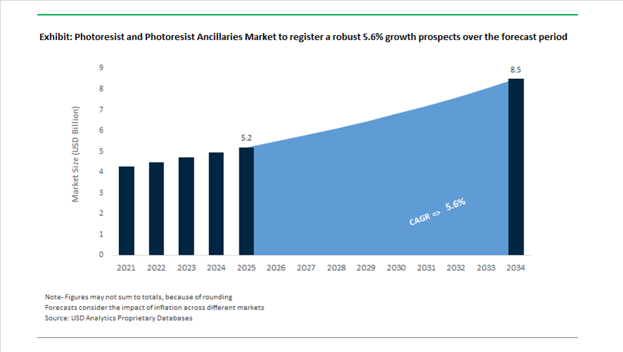
Photoresist and Photoresist Ancillaries Market Size 2025–2034: $5.2 Billion to $8.5 Billion at 5.6% CAGR Fueled by High-NA EUV, AI Chip Fabrication, and Advanced Packaging
The global photoresist and photoresist ancillaries market is projected to grow from $5.2 billion in 2025 to $8.5 billion by 2034, registering a CAGR of 5.6%. Market expansion is driven by accelerating demand for EUV photoresists, ArF immersion resists, dry film resists, CMP slurries, photoresist developers, underlayers, and post-CMP cleaning chemistries used in advanced semiconductor manufacturing. The proliferation of generative AI processors, High-Bandwidth Memory (HBM), automotive electrification, and 2nm and sub-2nm logic nodes is intensifying the need for ultra-high-purity lithography materials compatible with High-NA EUV systems. As semiconductor process geometries shrink, ancillary materials such as developers, rinse solutions, anti-reflective coatings, and underlayers are becoming equally critical to yield optimization and defect control.
Strategic restructuring in Japan in 2024 reshaped long-term competitive dynamics. In June 2024, JSR Corporation was privatized following a $6.4 billion acquisition by Japan Investment Corporation, culminating in its delisting in December 2024. This move enables JSR to pursue long-term semiconductor material investments without public market constraints, reinforcing its position in EUV photoresist innovation. In April 2024, Shin-Etsu Chemical committed ¥83 billion to construct a new production base in Gunma Prefecture, its first new domestic facility in over five decades, focused on EUV photoresists and related materials with completion targeted for 2026. The investment reflects Japan’s strategy to strengthen domestic semiconductor supply resilience amid geopolitical risk.
Capacity expansion in advanced lithography materials accelerated through 2024 and 2025. Fujifilm announced a ¥20 billion investment in September 2024 to expand EUV resist production at Shizuoka and increase post-CMP cleaner capacity by 40% at Oita, with phased operations through 2025 and 2026. In February 2025, Fujifilm committed €25 million to its Belgium facility to scale CMP slurry and photoresist developer production for European semiconductor and automotive electronics markets. In early 2024, Sumitomo Chemical commenced operations at its new Iksan plant in South Korea, creating a dual-site supply model for ArF and EUV photoresists to serve major Korean foundries with enhanced supply security.
High-NA EUV deployment in 2025 marked a structural inflection point for advanced photoresist demand. In late December 2025, Intel operationalized the world’s first commercial High-NA EUV systems at Fab 52 in Arizona, requiring new generations of photoresists and underlayers optimized for 0.55 NA lithography. Concurrently, Samsung installed its first ASML Twinscan EXE:5000 High-NA EUV tool at Hwaseong in early 2025, initiating validation of next-generation molecular resists for its planned 1.4nm node commercialization. These milestones substantially increase demand for chemically amplified EUV resists with higher resolution, lower line-edge roughness, and improved etch resistance.
Product innovation in ancillaries is accelerating in parallel with resist evolution. In March 2025, DuPont launched Riston® DI9500M and FD3000M dry film photoresists engineered for ultra-fine-line circuitry in AI servers and electric vehicle systems. In February 2026, Tokyo Ohka Kogyo upgraded its FY2025 earnings guidance citing robust AI-driven demand for advanced photoresists. The company also revised its Medium-Term Plan 2027 to accelerate capital expenditure in photoresist ancillary production, particularly for Fan-Out Wafer-Level Packaging (FOWLP) and advanced packaging technologies critical for heterogeneous integration.
Technology-Driven Trends and High-Conviction Opportunities in the Photoresist and Photoresist Ancillaries Market
Accelerated Adoption of EUV Photoresists and Strategic Ecosystem Lock-In
The global photoresist and photoresist ancillaries market is undergoing a decisive structural shift as semiconductor manufacturing transitions toward High-NA EUV lithography for sub-2nm logic and advanced memory nodes. At this level of miniaturization, photoresists are no longer interchangeable consumables but yield-critical materials embedded deep within the chipmaking ecosystem. Leading foundries including Intel, TSMC, and Samsung are therefore moving away from spot procurement toward long-term, technically co-developed supply agreements with a limited circle of qualified suppliers, primarily based in Japan and the United States.
By mid-2025, High-NA EUV tools had entered pilot production at multiple advanced fabs, forcing a material transition from conventional chemically amplified resists to Metal-Oxide Resists (MOR). These MOR systems deliver superior line-edge roughness control and reduced stochastic defects at extreme resolutions. A notable milestone occurred in September 2025, when JSR Corporation, through its subsidiary Inpria, successfully integrated metal-oxide photoresists with Lam Research’s dry resist processing technology. This integration materially reduced electron blur effects that had constrained yield at sub-5nm patterning, reinforcing MOR as the reference material class for future EUV generations.
The capital intensity of this transition is reshaping market economics. In 2024, EUV photoresists accounted for roughly 25% of total advanced lithography chemical revenues. This share is projected to exceed 45% by 2034 as High-NA adoption accelerates. The U.S. CHIPS Act has further entrenched supplier lock-in by catalyzing multi-billion-dollar EUV investments from Intel and Samsung, creating production environments where only SEMI-standard, ultra-high-purity resist ecosystems are technically viable. In parallel, Samsung Semiconductor confirmed in 2025 that EUV lithography had been fully deployed across its latest DRAM roadmap, increasing consumption of 13.5 nm wavelength-optimized resists that deliver materially higher resolution than legacy 193 nm DUV systems.
Diversification Toward Photoresists for Advanced Packaging and Heterogeneous Integration
As traditional 2D transistor scaling slows, value creation in semiconductors is increasingly shifting toward Advanced Packaging, including 2.5D interposers, 3D stacking, and chiplet architectures. This transition has elevated photoresists from a front-end process enabler to a critical back-end performance driver. Advanced packaging workflows require thick-film photoresists with high depth-of-focus, exceptional adhesion, and the ability to pattern complex redistribution layers and through-silicon vias under non-ideal substrate conditions.
By late 2025, equipment suppliers such as Heidelberg Instruments reported accelerating adoption of maskless lithography platforms, including the MLA 300 series, for adaptive precision patterning. These systems are increasingly used to define redistribution layer features below 2 microns, particularly in Fan-Out Wafer Level Packaging, where wafer warpage and topography variability demand resist systems with robust process windows. This has driven demand for specialty thick-film resists that can maintain dimensional fidelity across high aspect ratios while remaining compatible with modified FEOL lithography tools repurposed for backend interconnect fabrication.
The complexity of high-performance computing architectures has further blurred the boundary between FEOL and BEOL. Fine-pitch micro-bumping for HPC and AI accelerators now requires photoresists capable of supporting interconnect densities previously reserved for transistor layers. As a result, resist suppliers are increasingly developing hybrid portfolios that span EUV front-end resists and advanced packaging formulations, strengthening account stickiness and expanding wallet share per fab.
Specialty Photoresists for Next-Generation Micro-LED Display Manufacturing
Micro-LED technology represents one of the most attractive greenfield opportunities for the photoresist market, particularly in AR/VR devices, premium automotive displays, and next-generation wearables. Unlike OLED, Micro-LED fabrication relies on complex mass-transfer processes that require photoresists to function as temporary adhesives, sacrificial layers, and high-precision alignment aids rather than purely patterning materials.
During 2024–2025, equipment leaders such as ASMPT commercialized laser-based mass transfer platforms like the LT300Pro, capable of transferring approximately 9,000 Micro-LED dies per second. These processes impose extreme thermal and mechanical stress on photoresist materials, requiring formulations that can withstand high-energy laser exposure while maintaining sub-micron placement accuracy. This has created a premium niche for chemically robust, optically transparent photoresists engineered specifically for Micro-LED workflows.
As Micro-LED adoption expands beyond pilot programs, particularly following indications of high-end smartwatch and automotive HUD integration during 2025–2026, demand is rising for encapsulation and sacrificial resists tailored to transparent and curved display architectures. These applications offer structurally higher margins than mainstream semiconductor resists due to customization intensity and limited supplier qualification.
High-Purity Photoresist Ancillaries for China’s Mature-Node Fab Expansion
While global headlines focus on EUV, a parallel and structurally significant opportunity is emerging in China’s rapid expansion of mature-node semiconductor capacity. Nodes ranging from 28 nm to 45 nm are seeing sustained investment for automotive electronics, industrial IoT, and power management ICs. This expansion is generating robust, non-cyclical demand for photoresist ancillaries, including developers, strippers, and bottom anti-reflective coatings, which are indispensable for high-volume manufacturing.
According to TrendForce data published in October 2024, Chinese foundries are expected to drive approximately 6% growth in global mature-process capacity in 2025. By year-end, domestic players are projected to control more than 25% of the global top-10 mature-node market, with particular strength in the 28 nm and 22 nm segments. These fabs rely heavily on stable, high-purity ancillaries to maintain yield consistency across large production volumes.
National policy has amplified this demand. Under “Made in China 2025” and the 14th Five-Year Plan, the government has set a target of achieving 50% self-sufficiency in semiconductor equipment and materials by 2025. This has unlocked billions in subsidies through state-backed investment vehicles, accelerating capacity expansion at foundries such as SMIC and Hua Hong. In response, international suppliers are reshaping their footprints. In November 2025, Sumitomo Chemical announced the acquisition of semiconductor process chemical bases in Taiwan and the United States, enabling localized delivery of integrated resist-plus-ancillary solution packages to both Chinese and global customers.
Photoresist and Photoresist Ancillaries Market Share and Segmentation Insights
ArF Immersion Photoresists Lead Advanced Lithography Materials Demand in Sub-7nm Semiconductor Manufacturing
ArF immersion photoresists accounted for 34.80% of the Photoresist and Photoresist Ancillaries Market by product type in 2025, reflecting their role as the primary lithography material used in advanced semiconductor manufacturing. These 193 nm photoresists enable high-resolution pattern transfer required for logic and memory nodes down to 7 nm through water immersion lithography technology. Leading semiconductor fabs rely heavily on ArF immersion processes for multiple critical layers in integrated circuit fabrication. In 2025, multi-patterning lithography expansion using LELE, SADP, and SAQP techniques is increasing photoresist consumption per wafer layer, as each additional patterning step requires separate resist coatings and processing cycles across advanced semiconductor manufacturing workflows.
Semiconductor and Integrated Circuit Production Drives Photoresist and Ancillary Material Consumption
Semiconductors and integrated circuits represented 58.60% of the Photoresist and Photoresist Ancillaries Market by application in 2025, reflecting the intensive use of lithography materials in advanced chip fabrication. Each semiconductor wafer requires between 50 and 100 photolithography layers, with every layer utilizing photoresists and ancillary materials such as anti-reflective coatings, developers, and edge bead removers. As chip architectures become more complex, demand for high-performance lithography materials continues to expand. In 2025, increasing node complexity and advanced wafer processing requirements are driving higher material consumption per wafer, with EUV lithography and multi-patterning ArF immersion processes requiring more resist material and specialized ancillaries than previous semiconductor technology generations.
Photoresist and Photoresist Ancillaries Market Competitive Landscape
The global photoresist and photoresist ancillaries market is advancing rapidly with EUV lithography adoption and AI-driven semiconductor scaling toward sub-3nm nodes. Competition centers on high-purity, low-defect materials, strategic consolidation, and capital-intensive R&D led by Japanese players dominating advanced lithography chemistries.
JSR Accelerates EUV Dry Resist and AI-Driven Polymer Innovation Through Strategic Collaborations
JSR Corporation operates under a ¥900 billion ($6.3 billion) acquisition by Japan Investment Corporation, enabling a long-term private-equity-backed growth strategy in semiconductor materials. The September 2025 collaboration with Lam Research focuses on EUV dry resist technology, replacing wet processes to enhance resolution at sub-3nm nodes. A November 2025 partnership with IBM integrates AI-driven materials discovery using high-performance computing for next-generation polymer design. The SPACIER platform applies machine learning and molecular simulation to accelerate development of advanced optical polymers and photoresists. The August 2024 acquisition of Yamanaka Hutech strengthens its portfolio in high-purity precursor chemicals for front-end semiconductor processing. Strategic direction combines AI-enabled innovation, EUV resist leadership, and portfolio expansion in high-purity lithography materials.
TOK Expands Advanced EUV Resist Portfolio with Strong Growth in Electronic Functional Materials
Tokyo Ohka Kogyo Co., Ltd. (TOK) maintains leadership in advanced lithography materials with strong exposure to EUV and ArF resist demand driven by AI semiconductor manufacturing. The February 2026 partnership with Irresistible Materials targets commercialization of multi-trigger EUV resists to reduce stochastic defects in advanced nodes. The company reported record financial performance in FY2025, with 16% growth in its Electronic Functional Materials segment. FY2026 guidance projects a 12.3% increase in this division, supported by expansion into semiconductor back-end materials including packaging resists and wafer handling system (WHS) materials. Approximately 70% of electronic material sales are derived from advanced materials such as ArF and EUV resists, reflecting a shift away from legacy lithography chemistries. Product strategy focuses on defect reduction, yield optimization, and advanced semiconductor process integration.
Shin-Etsu Strengthens Lithography Materials Supply Chain with Large-Scale Investment and Global Manufacturing Network
Shin-Etsu Chemical Co., Ltd. leverages its vertically integrated manufacturing model across silicon wafers and photoresists to secure supply chain control in semiconductor fabrication. The company is investing ¥83 billion ($550 million) in a new lithography materials R&D and production facility in Gunma, with completion targeted for 2026. Consolidated net sales reached ¥2.56 trillion in 2025, reflecting 6.1% year-on-year growth and strong specialty chemical margins. A high equity ratio of 82.7% supports self-financed expansion and flexible capital allocation toward PFAS-free photoresist development. The company operates 67 overseas production bases, ensuring localized supply and mitigation of geopolitical risks. Strategic focus emphasizes high-purity photoresists, environmental compliance, and resilient global semiconductor material supply chains.
Fujifilm Scales Semiconductor Materials with AI-Enabled Inspection and PFAS-Free Photoresist Innovation
Fujifilm Electronic Materials has transformed into a high-growth supplier of integrated semiconductor processing solutions. The completion of a ¥13 billion advanced development facility in Shizuoka (November 2025) incorporates AI-based image recognition for fine particle inspection in high-purity photoresists. The company plans to invest over ¥100 billion between FY2025 and FY2026 to double semiconductor materials capacity by 2030, targeting AI data center demand. Product development includes PFAS-free photoresists and WAVE CONTROL MOSAIC™ color filter materials for advanced image sensors, contributing to 1.7x segment growth since 2021. The October 2024 investment in Oita expands post-CMP cleaner production by 40%, strengthening integration between photoresists and ancillary chemicals. Business strategy emphasizes one-stop semiconductor material solutions and high-purity process optimization.
Sumitomo Chemical Expands ArF Photoresist Capacity and Ancillary Integration for Advanced Lithography
Sumitomo Chemical Co., Ltd. is expanding global production capacity to meet rising demand for ArF immersion photoresists used in advanced 193nm lithography. New production lines at the Iksan Plant in South Korea and Osaka Works have increased advanced photoresist capacity by 250% compared to 2019 levels. The company holds a strong market position in ArF immersion resists critical for multi-patterning in memory and logic semiconductor devices. Proprietary organic synthesis capabilities support development of high-purity photoresist ancillaries, including developers and stripping solvents. Strategic alignment with Society 5.0 initiatives supports demand from ICT infrastructure and smart mobility applications. Production strategy integrates high-volume capacity expansion with advanced lithography material innovation.
Japan – EUV Leadership Anchored in Scale, AI, and Public–Private Integration
Japan remains the global benchmark for photoresist and photoresist ancillary innovation, underpinned by early commercialization of extreme ultraviolet technologies and tightly integrated supply ecosystems. In late 2025, JSR Corporation confirmed that its metal-based EUV resists had reached high-volume manufacturing readiness, aligning directly with 2 nm logic node requirements scheduled for 2026. Parallel capacity reinforcement is underway at Shin-Etsu Chemical, which disclosed substantial electronics materials capital expenditure in 2025 to expand ArF and EUV photoresist output at its Gunma and Niigata sites. These investments reinforce Japan’s role as the most reliable source of production-scale, high-purity photoresists.
Beyond scale, Japan is accelerating innovation velocity through digitalization and ancillary specialization. In November 2025, Tokyo Ohka Kogyo announced a collaboration with IBM to deploy generative AI for molecular-level resist discovery, with the explicit objective of cutting development timelines for KrF and ArF materials by half. Ancillary innovation is equally pronounced. Fujifilm launched high-resolution developers in October 2025 designed to suppress defectivity in advanced packaging and image sensor fabrication. These advances are reinforced by the government-backed Rapidus program, which entered its final equipment installation phase in late 2025 with on-site supply lines for ultra-high-purity ancillaries. Sustainability commitments further differentiate Japan, with leading producers pledging RE100 compliance for photoresist lines by 2026 under the Green Transformation policy.
South Korea – Localization Momentum and EUV Supply Chain Sovereignty
South Korea’s photoresist strategy is defined by rapid localization of advanced materials and deep integration with its semiconductor super-cluster agenda. In May 2025, Sumitomo Chemical, through its subsidiary Dongwoo Fine-Chem, announced an additional multi-billion won investment to construct a new cleanroom at its Iksan facility, with phased operations commencing in fiscal 2026. This expansion is directly aligned with replacing imported EUV and ArF resists in memory and logic fabs.
Domestic capability is maturing across the value chain. SK Materials Performance reported in late 2025 that its EUV photoresist portfolio had transitioned from pilot to production-ready status, supported by a roadmap to achieve net-zero operations across all resist lines by 2026. Government policy is reinforcing this trajectory. The 2025–2026 national budget includes targeted incentives for specialty electronic chemicals, explicitly covering photoresist removers and developers. Capacity diversification is further strengthened by JSR Corporation, which broke ground on a dedicated metal oxide resist plant in Korea during 2024–2025, targeting operations in 2026. Complementing manufacturing scale, Dongwoo Fine-Chem’s Pangyo Techno Valley R&D center became fully operational in early 2025, serving as a verification hub for next-generation EUV and ArF formulations.
China – Policy-Driven Substitution and Rapid Ancillary Localization
China’s photoresist market is being reshaped by mandatory localization policies and heavy public funding for advanced materials. In December 2025, Beijing began enforcing the so-called 50% rule, requiring new semiconductor capacity expansions to source at least half of equipment and materials domestically. This mandate has sharply accelerated adoption of locally produced photoresists and ancillaries. By late 2025, industry assessments indicated that China had reached approximately 50% self-sufficiency in photoresist removal and cleaning equipment, with Naura Technology emerging as a leading domestic supplier.
Financial backing is substantial and sustained. A dedicated allocation from the 344 billion yuan Big Fund Phase III is being directed toward ArF immersion and EUV photoresist research through 2026, reducing reliance on imported high-end materials. Regional specialization is also evident. Hubei Xingfa Group expanded its electronic-grade phosphorus and ancillary chemical lines in 2025 to support NAND and DRAM fabrication clusters. On the downstream side, Chinese formulators are pivoting toward dry film photoresists for fan-out wafer-level packaging, with commercial shipments to domestic OSAT providers beginning in the third quarter of 2025. Collectively, these measures are compressing the technology gap in ancillaries faster than in core EUV resist chemistries.
United States – CHIPS-Driven Capacity and Ultra-Purity Differentiation
The United States photoresist and ancillary landscape is being reconfigured by domestic fab construction and a renewed focus on purity leadership. Federal CHIPS Act incentives have catalyzed new ancillary production investments by DuPont and Entegris, aimed at supporting advanced fabs under construction in Arizona and Ohio. In parallel, portfolio rationalization is sharpening strategic focus. In September 2025, DuPont completed the divestiture of its aramids business, redeploying capital toward semiconductor technologies and high-purity photoresist systems.
Collaboration remains a defining feature of the U.S. ecosystem. In late 2025, Lam Research entered a cross-licensing agreement with JSR and Inpria to advance dry-resist technologies for EUV lithography, a critical enabler for next-generation logic manufacturing. Regulatory and standards leadership further differentiates the U.S. market. A 2025 National Institute of Standards and Technology report established new voluntary benchmarks for parts-per-quadrillion impurity control in photoresist developers, directly addressing contamination risks at 3 nm and below. This emphasis on ultra-purity positions U.S. suppliers at the premium end of the ancillary spectrum.
Comparative Snapshot – Photoresist and Ancillaries by Country
Photoresist and Photoresist Ancillaries Market County Level Snapshot
|
Country
|
Strategic Focus Area
|
Key 2025–2026 Differentiator
|
Industry Role
|
|
Japan
|
EUV leadership and integrated ecosystems
|
AI-driven resist design and RE100 manufacturing
|
Global technology benchmark
|
|
South Korea
|
Localization and memory-led scaling
|
EUV supply chain sovereignty and cleanroom expansion
|
Fast-rising regional hub
|
|
China
|
Policy-enforced substitution
|
Big Fund-backed ArF and ancillary localization
|
Scale-driven challenger
|
|
United States
|
Domestic capacity and purity leadership
|
CHIPS-driven investments and ppq impurity standards
|
Premium ancillary supplier
|
Photoresist and Photoresist Ancillaries Market Report Scope
Photoresist and Photoresist Ancillaries Market
|
Parameter
|
Details
|
|
Market Size (2025)
|
$5.2 Billion
|
|
Market Size (2034)
|
$8.5 Billion
|
|
Market Growth Rate
|
5.6%
|
|
Segments
|
By Product Type (ArF Immersion Photoresists, ArF Dry Photoresists, KrF Photoresists, EUV Photoresists, G-line & I-line Photoresists), By Ancillary Type (Anti-Reflective Coatings, Photoresist Developers, Photoresist Removers & Strippers, Edge Bead Removers, Hardmasks, Adhesion Promoters), By Application (Semiconductors & Integrated Circuits, Advanced Packaging, Printed Circuit Boards, Flat Panel Displays, MEMS & Image Sensors)
|
|
Study Period
|
2019- 2025 and 2026-2034
|
|
Units
|
Revenue (USD)
|
|
Qualitative Analysis
|
Porter’s Five Forces, SWOT Profile, Market Share, Scenario Forecasts, Market Ecosystem, Company Ranking, Market Dynamics, Industry Benchmarking
|
|
Companies
|
JSR Corporation, Tokyo Ohka Kogyo Co. Ltd., Shin-Etsu Chemical Co. Ltd., Fujifilm Holdings Corporation, DuPont de Nemours Inc., Sumitomo Chemical Co. Ltd., SK Materials Performance, Merck KGaA, Entegris Inc., Resonac Holdings Corporation, LG Chem Ltd., Allresist GmbH, Dongjin Semichem, Yuntianhua Group, Dainippon Screen Manufacturing Co. Ltd.
|
|
Countries
|
US, Canada, Mexico, Germany, France, Spain, Italy, UK, Russia, China, India, Japan, South Korea, Australia, South East Asia, Brazil, Argentina, Middle East, Africa
|
Photoresist and Photoresist Ancillaries Market Segmentation
By Product Type
- ArF Immersion Photoresists
- ArF Dry Photoresists
- KrF Photoresists
- EUV Photoresists
- G-line & I-line Photoresists
By Ancillary Type
- Anti-Reflective Coatings
- Photoresist Developers
- Photoresist Removers & Strippers
- Edge Bead Removers
- Hardmasks
- Adhesion Promoters
By Application
- Semiconductors & Integrated Circuits
- Advanced Packaging
- Printed Circuit Boards
- Flat Panel Displays
- MEMS & Image Sensors
By Region
- North America (United States, Canada, Mexico)
- Europe (Germany, France, United Kingdom, Spain, Italy, Rest of Europe)
- Asia Pacific (China, India, Japan, South Korea, Australia, Rest of APAC)
- South and Central America (Brazil, Argentina, Rest of SCA)
- Middle East and Africa (Saudi Arabia, UAE, South Africa, Rest of Middle East, Rest of Africa)
Top Companies in Photoresist and Photoresist Ancillaries Industry
- JSR Corporation
- Tokyo Ohka Kogyo Co. Ltd.
- Shin-Etsu Chemical Co. Ltd.
- Fujifilm Holdings Corporation
- DuPont de Nemours Inc.
- Sumitomo Chemical Co. Ltd.
- SK Materials Performance
- Merck KGaA
- Entegris Inc.
- Resonac Holdings Corporation
- LG Chem Ltd.
- Allresist GmbH
- Dongjin Semichem
- Yuntianhua Group
- Dainippon Screen Manufacturing Co. Ltd.
*- List not Exhaustive
