Market Snapshot - Signal Integrity, Energy Efficiency, and Node Scaling Are Structurally Expanding the Low Dielectric Materials Market
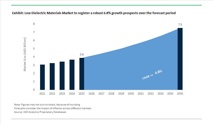
The Low Dielectric Materials Market is valued at USD 3.9 billion in 2025 and is projected to reach USD 7.5 billion by 2035, growing at a 6.8% CAGR as signal loss and power dissipation become first-order design constraints across communications, computing, and semiconductor manufacturing. As operating frequencies rise and feature sizes shrink, dielectric performance is no longer a secondary material attribute; it directly governs achievable data rates, energy efficiency, and system reliability.
Demand is being pulled by three structurally independent but technologically converging end markets. In 5G/mmWave infrastructure and automotive radar, material selection is dictated by strict loss budgets rather than cost alone. Base stations and 77 GHz radar modules increasingly require laminates with dissipation factors (Df) below ~0.003 at 10 GHz to keep signal attenuation under ~5% over practical trace lengths. This requirement now governs a majority of new high-frequency RF designs, effectively narrowing the material set to proven low-loss systems with stable dielectric behavior across temperature and humidity extremes.
In data-center networking and AI compute, low dielectric materials are becoming an energy-efficiency lever. High-speed serial links operating at 25 GHz and above demand substrates and PCB materials that maintain Df stability below ~0.001 to minimize insertion loss, jitter, and retransmission overhead. As rack-level power density increases, even marginal dielectric losses translate into meaningful thermal and energy penalties, elevating low-loss materials from premium options to architectural necessities in next-generation server and accelerator platforms.
At the semiconductor level, advanced packaging and node scaling are reinforcing long-term demand. As interconnect dimensions approach physical limits, enhanced low-dielectric materials paired with alternative wiring metals have demonstrated material reductions in interconnect resistance on the order of ~25% at leading-edge nodes, supporting higher performance per watt. In parallel, flexible electronics represent an outsized growth vector: liquid crystal polymer (LCP) and modified polyimide films are seeing rapid uptake in flexible PCBs, antennas, and wearable devices, with demand trajectories significantly outpacing the broader market as form factors diversify and operating frequencies climb.
Material competition within the market reflects trade-offs between ultimate performance and manufacturability. PTFE-based laminates continue to anchor the low-loss segment, retaining a substantial share due to their well-established dielectric stability across wide temperature ranges. At the same time, hydrocarbon-ceramic composites are gaining adoption where fabrication compatibility, multilayer processing, and cost efficiency influence OEM decisions. Over the forecast period, value capture will concentrate among suppliers that can deliver repeatable low-Dk/Df performance at scale, support advanced fabrication processes, and demonstrate reliability under real operating conditions. As digital infrastructure becomes increasingly frequency- and power-constrained, low dielectric materials are evolving into foundational enablers of next-generation connectivity and compute efficiency.
Market Analysis: Product Launches, Capacity Expansions and Node/Packaging Innovations
Industry activity over the past two years demonstrates simultaneous emphasis on material innovation for mmWave/automotive radar, flexible film development for wearables, and package-level advances that support semiconductor node scaling. In June 2024 Doosan Corporation Electro-Materials showcased next-generation mmWave antenna technologies and low-loss materials in collaboration with Movandi (BeamX platform), signalling early commercial efforts to scale small-cell deployments. July 2024 Panasonic Industry released low-dielectric multilayer resin materials targeted at high-speed servers and AI compute devices, anticipating growing thermal and wiring density requirements.
Momentum accelerated in 2025 as suppliers rolled new chemistries and expanded capacity to meet immediate 5G and packaging demand. In May 2025, 3M launched a lightweight low-dielectric polymer composite for aerospace and satellite components to improve high-frequency RF transfer and lower signal attenuation. May 2025 also saw Toray form a strategic partnership with a major semiconductor supplier to commercialize low-dielectric glass-fiber reinforced materials for next-generation packaging substrates - explicitly targeting 5G/6G frequencies and high-density interposers. June 2025 Rogers Corporation introduced an ultra-low Dk/Df family engineered for millimetre-wave antennas and automotive radar, while June 2025 Mitsui Chemicals advanced a low-Dk polymer film for high-frequency flexible printed circuits (FPCs) with pilot production addressing smartphone and wearable OEMs. In July 2025 DuPont Electronics & Industrial expanded low-Dk laminate production to secure higher volumes for 5G infrastructure and advanced packaging. Most recently, December 2025 Denka launched SNECTON, a new low-dielectric organic insulating resin tailored for next-generation high-speed communications, reinforcing the continual arrival of specialty chemistries to the market.
Low Dielectric Materials Market Trends and Opportunities
Market Trend 1: Ultra-Low-Loss Thermoset Polymers Replacing FR-4 in 5G mmWave and Early 6G Infrastructure
The rapid commercialization of 5G mmWave and the forward push toward sub-THz 6G bands are fundamentally altering dielectric material selection, accelerating the replacement of conventional FR-4 with ultra-low-loss thermoset polymers engineered for frequencies above 26 GHz. As signal attenuation scales with the square of operating frequency, even marginal dielectric losses translate into substantial degradation in antenna efficiency and system-level power budgets. In response, materials such as modified polyphenylene ether (mPPE) are being increasingly specified due to their tightly controlled dielectric constant and consistently low dissipation factors across wide frequency bands. Asahi Kasei’s 2025 technical disclosures highlight that mPPE-based laminates suppress surface-wave entrapment, directly improving radiation efficiency in 5G base station radomes, dielectric resonators, and phased-array antenna substrates. Importantly, the industry is favoring thermoset systems over PTFE for large-scale telecom deployments. While PTFE remains indispensable for niche ultra-high-frequency applications, it poses challenges in multilayer PCB fabrication due to poor adhesion, drilling complexity, and higher scrap rates. Low-loss thermosets bridge this gap by offering PTFE-adjacent electrical performance while remaining compatible with standard PCB manufacturing lines. This shift is visible in the mobile device ecosystem as well: in 2024, Zhen Ding Tech Group partnered with a leading smartphone OEM to co-develop ultra-thin RF PCBs using advanced low-Dk laminates that support foldable form factors and AI-driven antenna tuning. Collectively, these developments indicate that low dielectric thermosets are no longer specialty materials but foundational enablers of scalable high-frequency connectivity.
Market Trend 2: Adoption of Spin-On and CVD Ultra-Low-k Dielectrics in Sub-3nm Logic Nodes
At the leading edge of semiconductor fabrication, the industry’s ability to sustain performance scaling is increasingly constrained by interconnect delay rather than transistor switching speed. As metal pitches shrink at 3nm and below, parasitic capacitance between copper lines has emerged as a dominant limiter of power efficiency and clock frequency. This has driven foundries toward porous, ultra-low-k dielectrics with dielectric constants below 2.5, deposited via spin-on or plasma-enhanced CVD processes. In March 2025, Applied Materials introduced enhancements to its Black Diamond™ PECVD platform, specifically engineered to address the mechanical fragility that historically plagued porous ULK films during aggressive plasma etch and CMP steps. These next-generation formulations mitigate film collapse and cracking, enabling reliable integration at 3nm and future 2nm nodes. TSMC has confirmed that its N3 high-volume manufacturing process incorporates advanced low-k copper interconnect stacks, with subsequent N3E and N3X variants leveraging further ULK refinements to deliver measurable gains in power efficiency and switching speed over 5nm technology. Beyond traditional SiCOH chemistries, industry research cited in 2025 points to emerging material classes such as boron carbide and boron nitride dielectrics. These alternatives aim to push effective k-values toward ~2.3 while retaining sufficient Young’s modulus to survive back-end-of-line processing. This convergence of materials science and process integration underscores how low dielectric materials have become strategic levers for extending Moore’s Law in the AI era.
Market Opportunity 1: Low-Dk, Low-CTE Mold Compounds for Fan-Out Wafer-Level Packaging (FO-WLP)
The rapid adoption of fan-out wafer-level packaging for heterogeneous integration is creating a structurally important opportunity for low-dielectric, low-CTE epoxy mold compounds. As package sizes scale and redistribution layers become denser, FO-WLP platforms are increasingly vulnerable to warpage driven by thermal expansion mismatch between silicon and conventional mold materials. A 2025 technical analysis of large-panel FO-WLP processes highlights that standard mold compounds, with CTE values exceeding 20 ppm/°C, induce significant curvature when paired with silicon’s ~3 ppm/°C expansion rate. This has elevated demand for EMC formulations containing 60–70% spherical silica fillers, capable of reducing CTE below 12 ppm/°C while maintaining mechanical robustness. At the same time, RF performance requirements are tightening sharply. Automotive radar at 77 GHz and 5G mmWave modules now require mold compounds with dielectric constants below 3.2 and dissipation factors under 0.004 at 10 GHz—thresholds that are 20–30% more stringent than those used in 4G-era packaging. Leading OSATs in Taiwan are already specifying these advanced EMCs across the majority of their FO-WLP lines. However, the availability of high-purity spherical silica has emerged as a bottleneck, with lead times stretching to 26 weeks in late 2024. This supply constraint creates a clear opening for localized producers of ultra-pure quartz and engineered fillers in Japan and North America to lock in long-term, high-margin supply agreements with packaging houses.
Market Opportunity 2: Low-Dielectric Materials for Co-Packaged Optics in AI Data Centers
As hyperscale data centers transition toward 1.6T and 3.2T networking architectures, co-packaged optics is emerging as a structural shift in system design—one that places unprecedented demands on dielectric materials. Traditional pluggable optical modules are approaching a power-density ceiling due to long electrical traces between switch ASICs and optical engines, a challenge widely referred to as the SerDes “power wall.” CPO architectures overcome this by integrating optics directly alongside the ASIC, but doing so requires interposer and substrate materials with ultra-low electrical and optical losses, high thermal stability, and compatibility with 2.5D/3D integration. At GTC 2025, NVIDIA unveiled its Spectrum X and Quantum X photonics platforms, built on TSMC’s SoIC technology, which relies on advanced dielectric stacks to minimize signal degradation as optical engines are brought closer to high-power switching silicon. IDTechEx reports from late 2025 indicate that advanced hydrocarbon polymers and colorless polyimides are increasingly favored in these architectures, as they reduce power consumption while maintaining dimensional stability under elevated operating temperatures. Policy support is reinforcing this opportunity: in December 2025, India announced a targeted Electronics Components Manufacturing Scheme aimed at domestic production of high-speed PCBs and advanced packaging materials, explicitly including low-Dk substrates for telecom and data-center interconnects. Together, AI-driven bandwidth growth and sovereign electronics initiatives are positioning low dielectric materials as critical infrastructure enablers rather than niche semiconductor inputs.
Market Share Analysis: Low Dielectric Materials Market
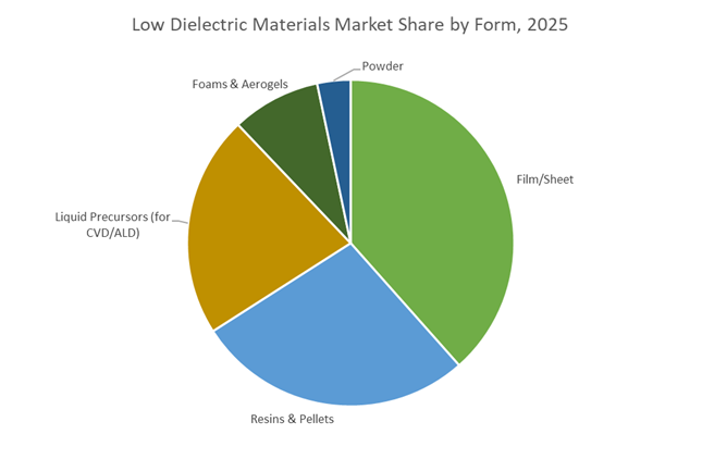
Market Share by Form: Low-Dielectric Films and Sheets as the Backbone of Ultra-High-Speed PCB Architectures
Low-dielectric films and sheets account for roughly 35% of the Low Dielectric Materials Market because they sit at the core of next-generation, high-layer-count printed circuit boards required for 5G, early-stage 6G, hyperscale data centers, and advanced radar systems. Their dominance is not volume-driven insulation demand but signal-integrity economics: as data rates cross the 112 Gbps to 224 Gbps per channel threshold, even marginal dielectric instability translates into exponential signal loss, heat generation, and power inefficiency. Advanced film-based laminates such as MEGTRON-class materials remain indispensable because they combine tight dielectric constant control (≈2.94 ±0.04 at 10 GHz) with ultra-low dissipation factors, enabling phase stability across long trace lengths and dense multilayer stacks. The segment’s share is further reinforced by process survivability, as leading low-k films now tolerate >300°C lamination and reflow cycles, allowing compatibility with high-speed PCB manufacturing without deformation or resin bleed. Critically, films and sheets also enable loss-optimized copper interfaces—when paired with H-VLP copper foils, they reduce insertion loss by up to 20%, directly lowering power draw in network equipment. This combination of data-rate scalability, manufacturing compatibility, and predictable electrical performance explains why film and sheet formats remain the structural foundation of the low-dielectric materials market rather than being displaced by bulk resins or coatings.
Market Share by Application: Telecommunications as the Signal-Integrity Demand Engine
Telecommunications represents approximately 35% of total low-dielectric material demand, making it the largest and most strategically influential application segment. This leadership is structurally tied to the physics of high-frequency transmission rather than cyclical capex alone. As 5G mmWave and massive-MIMO architectures proliferate, base stations and antenna systems operate at frequencies where dielectric loss, moisture absorption, and phase noise become limiting factors for network economics. High-performance low-k materials deliver tangible system-level advantages, including up to 3 dB signal-gain improvements, effectively doubling coverage radius and reducing tower density—one of the most expensive line items for telecom operators. The segment’s share is further secured by long-duration reliability requirements: telecom infrastructure is now designed for 10+ years of continuous operation, often in harsh outdoor environments, driving demand for materials with near-zero moisture absorption (<0.02%) to prevent signal drift and uptime degradation. As networks evolve toward higher bandwidth aggregation and early 6G research, ultra-low dissipation factors (~0.0008 at 10 GHz) have become non-negotiable specifications, locking low-dielectric materials into the core of RF front-end and backhaul design. Consequently, telecommunications remains the primary commercialization pathway where performance gains translate directly into lower operating costs, fewer assets per square kilometer, and higher network reliability, sustaining its leading market share within the low-dielectric materials ecosystem.
Competitive Landscape: Incumbent Laminate Specialists, Polymer Majors and Specialty Chemical Players Dominating Low-Dk Roadmaps
The competitive field mixes PCB laminate specialists, polymer and fluoropolymer producers, and large petrochemical firms supplying resin precursors. Market leaders differentiate on ultra-low Dk/Df capability, frequency/thermal stability, flexible-film platforms (LCP/polyimide), package-grade substrate alliances, and scale-backed global supply chains for telecom and data-center customers.
Dupont Electronics & Industrial - Flexible-Circuit Leader Supplying Low-Loss Polyimide/LCP Films and Expanded Low-Dk Laminate Capacity
DuPont is a global leader in flexible circuit materials (Pyralux®) and low-loss laminates. The company’s polyimide and LCP film products are widely used for 77 GHz automotive radar and 5G handset antennas because of dimensional and thermal stability. In July 2025 DuPont expanded production of low-Dk laminates to reinforce supply for 5G infrastructure and advanced semiconductor packaging-demonstrating a strategic commitment to high-growth digital infrastructure and mission-critical PCB applications. DuPont also provides hydrocarbon laminate alternatives to PTFE for applications that require stable dielectric constants across temperature and frequency.
Rogers Corporation - High-Frequency Laminate Specialist Focused On Mmwave and Automotive Radar Performance
Rogers is a globally recognised specialist in high-frequency circuit materials (RO3003® family), delivering tightly controlled Dk tolerances (e.g., 3.00±0.04 at 10 GHz) required for mmWave 5G and radar modules. In June 2025 Rogers introduced a new ultra-low Dk/Df family engineered specifically for millimetre-wave antennas and automotive radar systems, reinforcing its leadership where thermal stability and low loss are mandatory. Rogers’ products underpin more than 90% of global automotive radar modules and the company pursues close co-development with OEMs and Tier-1 suppliers to customise dielectric stacks for high-speed digital and RF subsystems.
SABIC - Polymer and Resin Scale For Cost-Competitive, High-Volume Low-Dk Solutions (M-PPE, COC)
SABIC brings petrochemical scale to low-dielectric polymers such as modified polyphenylene ether (m-PPE) and cyclic olefin copolymer (COC), offering a balance of low Dk/Df with robust thermal and mechanical performance for PCB substrates. Its NORYL resin systems are used in copper-clad laminates (CCL) for high-frequency boards and data-center applications, and SABIC’s global petrochemical footprint enables cost-competitive, geographically diversified supply - a key advantage for high-volume electronics manufacturers and infrastructure deployments.
Asahi Kasei Corporation - Specialty Polymer Developer Focused On M-PPE and Polyimide Films For 5G Components
Asahi Kasei focuses on high-performance specialty polymers (m-PPE, polyimide) and R&D for thermal stability-critical for high-frequency PCBs subject to localized heating from high data-rate processing. Its film and resin solutions support high-density wiring and miniaturised multi-layer PCBs in Asia-Pacific’s electronics manufacturing base. The company’s materials are optimized to maintain dielectric integrity in compact, high-layer-count server and handset boards.
Arkema - Fluoropolymer and LCP/Polyimide Investments For Radomes, Cable Insulation and Future 6G Substrates
Arkema is a fluoropolymer leader (Kynar® PVDF) offering inherently low Dk/Df materials used in high-frequency wire & cable insulation and radomes for aerospace/defense. Arkema has been developing ultra-low loss RF materials and is investing in LCP and polyimide film capabilities to capture growth in flexible low-loss substrates for 6G R&D and advanced telecommunications. Its portfolio addresses both radome transparency and mechanical durability needs in demanding defense and satellite applications.
South Korea has emerged as a global epicenter for low dielectric and ultra-low-k materials, driven by its ambition to dominate AI semiconductor packaging and HBM4 architectures. In December 2025, the government announced a ₩700 trillion (≈US$520 billion) long-term semiconductor investment plan to 2047, with the Southern Semiconductor Innovation Belt—linking Gwangju, Busan, and Gumi—designated as the nucleus for advanced packaging and materials qualification. Gwangju’s role as the official packaging hub is accelerating domestic scale-up of polyimide (PI) and liquid crystal polymer (LCP) dielectric films engineered for extreme thermal and electrical stability.
Material innovation is tightly coupled with process demands. Under the ₩360.6 billion advanced packaging mandate (to 2031) led by MOTIE, South Korea is fast-tracking ultra-low-dielectric PI films capable of surviving 260 °C reflow cycles required for HBM4 and NPU integration. In late 2025, PI Advanced Materials received ministerial recognition for breakthroughs in high-heat-resistant, low-loss PI films used across EV battery management systems and 5G/6G hardware, reinforcing Korea’s materials-to-packaging sovereignty.
Japan: GX 2040 Vision Anchors Low-Carbon, High-Frequency Dielectrics
Japan continues to lead the high-purity resin and precursor segments of the low dielectric materials market, aligning semiconductor growth with decarbonization under the GX 2040 Vision approved on January 18, 2025. The strategy prioritizes semiconductors and data centers as national growth engines and allocates R&D subsidies to producers using low-carbon energy and chemically efficient synthesis routes for next-generation dielectrics.
In 2025, Japanese majors such as Mitsubishi Gas Chemical and Asahi Kasei expanded output of Cyclic Olefin Copolymers (COC) and Cyanate Ester resins, targeting 6G signal reflectors and transparent reflect-arrays operating at terahertz frequencies. Downstream demand is scaling: Kyocera and TDK expanded Kagoshima plants (late-2024/early-2025) to boost MLCCs and high-frequency dielectric substrates for ADAS and automotive radar, cementing Japan’s leadership in low-loss, high-reliability dielectrics.
United States: CHIPS Act Pull-Through and Reshore-to-Scale Materials Strategy
The United States low dielectric materials market is being reshaped by CHIPS Act-driven reshoring and defense-grade supply-chain security. In March 2025, the Department of Commerce established the Investment Accelerator, streamlining approvals for >$1 billion projects tied to critical intermediates, including fluoropolymers (PTFE) and modified polyphenylene ether (m-PPE) used in high-frequency PCBs and AI server backplanes.
Trade dynamics accelerated localization. Tariff escalations in Spring 2025 on specialty polymers imported from Germany and Belgium pushed U.S. PCB manufacturers toward domestic suppliers such as Huntsman Corporation and Dow. Technology co-evolution is visible at the node level: in July 2024, Applied Materials unveiled ruthenium wiring for 2 nm nodes, designed to operate in tandem with ultra-low-k dielectrics to cut electrical resistance by ~25%, a prerequisite for energy-efficient AI data centers scaling in 2025.
China: Export Controls, 5G Density, and Dielectric Indigenization
China is leveraging its whole-chain governance of electronic precursors while accelerating self-sufficiency in high-end dielectric resins. Effective November 2025, MOFCOM implemented new export licensing for rare-earth metals and superhard materials, indirectly constraining global access to ceramic and metallic inputs used in hybrid dielectric composites.
Domestic capacity is rising in parallel. The MIIT 2025–2027 Action Plan mandates a 2.5% R&D-to-GDP ratio, catalyzing localized clusters for 5G/6G-grade PTFE and LCP with a goal of 70% domestic content for basic semiconductor materials by end-2025. Infrastructure demand is intense: China’s dense 5G base-station rollout is driving sustained uptake of low-loss laminates and radome materials, while domestic production of high-performance chemical fibers grew 5.6% in 2025, reinforcing scale-led indigenization.
Taiwan: Sub-2 nm Nodes and Ultra-Low-k Validation at Scale
Taiwan remains the global proving ground for ultra-low-k (ULK) materials, dictated by the sub-2 nm roadmaps of TSMC and national research bodies. At IEDMS 2025 (Hsinchu, October), researchers presented naphthalene-based poly(ester-imide)s achieving Df < 0.0020 at 10 GHz, among the lowest reported for 6G-class hardware.
Policy and research reinforce manufacturability. In December 2025, Taiwan’s MOEA highlighted 15 advanced material technologies, including dielectric metamaterials for flexible, transparent 6G antennas embedded into urban glass façades. Meanwhile, Industrial Technology Research Institute is piloting air-gap insulation in 3D-stacked chips, dramatically reducing interconnect capacitance—an approach expected to become standard for sub-2 nm heterogeneous integration by 2026.
India: Semicon India Creates Structural Pull for Low-Loss Dielectrics
India is rapidly transitioning into a manufacturing base for electronics-grade dielectric substrates, driven by policy-induced infrastructure pull. By October 2025, the PLI scheme for large-scale electronics had attracted ₹14,065 crore in investments, while the Electronics Components Manufacturing Scheme (ECMS) targeted domestic production of HDI PCBs requiring low-loss resins and underfills.
The Semicon India Programme amplified demand. In December 2025, MeitY confirmed approval of 10 semiconductor units totaling ₹1.6 lakh crore (≈US$19 billion), primarily in assembly, testing, and packaging (ATP)—creating immediate demand for locally sourced low-dielectric materials. Talent development is scaling in tandem: the Chips-to-Startup (C2S) initiative now supports 397 universities with EDA tools and materials grants, focusing on fluorinated polyimides and BT resins, positioning India as a future low-k materials ecosystem rather than a pure end-market.
2025 Strategic Matrix: Low Dielectric Materials by Country
Low Dielectric Materials Matrix
|
Country
|
Primary Market Driver
|
2025 Strategic Milestone
|
Key Material Focus
|
|
South Korea
|
AI & HBM4 packaging
|
₩700T semiconductor roadmap
|
Polyimide (PI), LCP
|
|
Japan
|
6G & GX 2040
|
GX strategy approval (Jan 2025)
|
COC, cyanate ester, ceramics
|
|
United States
|
AI data centers & CHIPS
|
Investment Accelerator launch
|
m-PPE, PTFE, ULK stacks
|
|
China
|
5G scaling & indigenization
|
MOFCOM export controls (Nov 2025)
|
LCP, PTFE, ceramic hybrids
|
|
Taiwan
|
Sub-2 nm integration
|
IEDMS 2025 ULK breakthrough
|
ULK polymers, air-gaps
|
|
India
|
Electronics PLI & ATP
|
₹1.6 L cr Semicon approvals
|
HDI PCB & BT resins
|
Low Dielectric Materials Market Report Scope
Low Dielectric Materials Market
|
Parameter
|
Details
|
|
Market Size (2025)
|
$3.9 Billion
|
|
Market Size (2035)
|
$7.5 Billion
|
|
Market Growth Rate
|
6.8%
|
|
Segments
|
By Material (Fluoropolymers, Modified PPE, Polyimide, COC, LCP, Cyanate Ester, Ceramics & LTCC, Ultra-Low-k Dielectrics), By Network Structure (Organic Network, Inorganic Network, Hybrid & Porogen Precursors), By Form (Film/Sheet, Resins & Pellets, Foams & Aerogels, Powder, Liquid Precursors), By Processing Technology (CVD/PECVD, Spin-on Dielectric, ALD, PVD), By Application (Printed Circuit Boards, Antennas, Semiconductor Packaging, Radomes & RF Enclosures, Wire & Cable Insulation, Capacitors & MEMS Devices), By End-User Industry (Telecommunications, Data Centers & Computing, Consumer Electronics, Automotive, Aerospace & Defense)
|
|
Study Period
|
2019- 2024 and 2025-2034
|
|
Units
|
Revenue (USD)
|
|
Qualitative Analysis
|
Porter’s Five Forces, SWOT Profile, Market Share, Scenario Forecasts, Market Ecosystem, Company Ranking, Market Dynamics, Industry Benchmarking
|
|
Companies
|
DuPont de Nemours Inc., Rogers Corporation, Panasonic Industry Co. Ltd., Mitsui Chemicals Inc., Asahi Kasei Corporation, Toray Industries Inc., Sumitomo Chemical Co. Ltd., SABIC, BASF SE, Mitsubishi Chemical Corporation, Shin-Etsu Chemical Co. Ltd., 3M Company, Arkema S.A., Zeon Corporation, Huntsman Corporation
|
|
Countries
|
US, Canada, Mexico, Germany, France, Spain, Italy, UK, Russia, China, India, Japan, South Korea, Australia, South East Asia, Brazil, Argentina, Middle East, Africa
|
Low Dielectric Materials Market Segmentation
By Material
- Fluoropolymers
- Modified Polyphenylene Ether (mPPE)
- Polyimide (PI)
- Cyclic Olefin Copolymer (COC)
- Liquid Crystal Polymer (LCP)
- Cyanate Ester
- Ceramics & Low-Temperature Co-fired Ceramics (LTCC)
- Ultra-Low-k (ULK) Dielectrics
By Network Structure
- Organic Network
- Inorganic Network
- Hybrid & Porogen Precursors
By Form
- Film/Sheet
- Resins & Pellets
- Foams & Aerogels
- Powder
- Liquid Precursors (CVD/ALD applications)
By Processing Technology
- Chemical Vapor Deposition (CVD/PECVD)
- Spin-on Dielectric / Spin Coating
- Atomic Layer Deposition (ALD)
- Physical Vapor Deposition (PVD)
By Application
- Printed Circuit Boards
- Antennas
- Semiconductor Packaging
- Radomes & RF Enclosures
- Wire & Cable Insulation
- Capacitors & MEMS Devices
By End-Use Industry
- Telecommunications
- Data Centers & Computing
- Consumer Electronics
- Automotive
- Aerospace and Defense
By Region
- North America (United States, Canada, Mexico)
- Europe (Germany, France, United Kingdom, Spain, Italy, Rest of Europe)
- Asia Pacific (China, India, Japan, South Korea, Australia, Rest of APAC)
- South and Central America (Brazil, Argentina, Rest of SCA)
- Middle East and Africa (Saudi Arabia, UAE, South Africa, Rest of Middle East, Rest of Africa)
Top Companies in Low Dielectric Materials Market
- DuPont de Nemours, Inc.
- Rogers Corporation
- Panasonic Industry Co., Ltd.
- Mitsui Chemicals, Inc.
- Asahi Kasei Corporation
- Toray Industries, Inc.
- Sumitomo Chemical Co., Ltd.
- SABIC
- BASF SE
- Mitsubishi Chemical Corporation
- Shin-Etsu Chemical Co., Ltd.
- 3M Company
- Arkema S.A.
- Zeon Corporation
- Huntsman Corporation
*- List not Exhaustive
