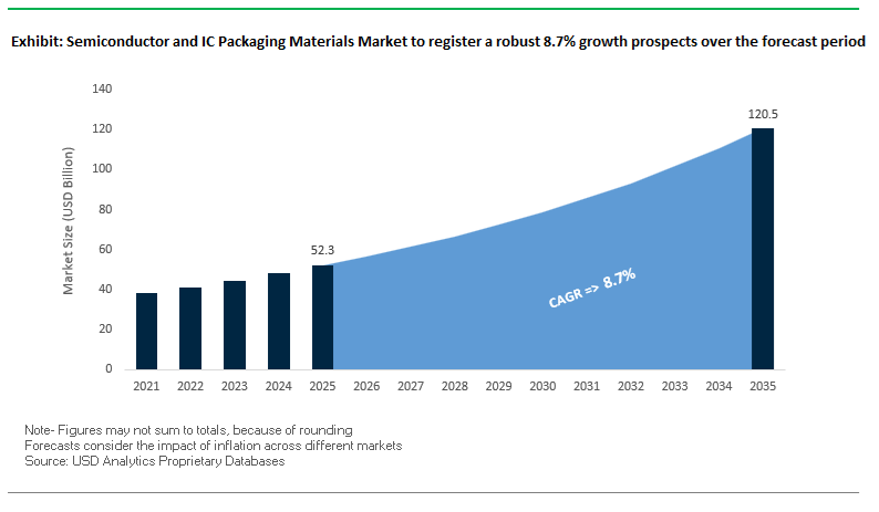
The Semiconductor and IC Packaging Materials Market is valued at USD 52.3 billion in 2025, expected to reach USD 120.4 billion by 2035, growing at a robust CAGR of 8.7%. The momentum is driven by the transition from conventional 2D packaging toward advanced Heterogeneous Integration (HI), chiplet architectures, 2.5D/3D packaging, and high-performance computing (HPC) platforms.
The semiconductor sector is undergoing its most significant structural transformation in decades, driven by AI compute proliferation, high-bandwidth memory (HBM) adoption, chiplet-based architectures, EV power electronics, and 5G infrastructure expansion. These macro trends have shifted material demand from traditional, low-end packaging inputs to ultra-high-performance hybrid polymers, resins, substrate films, and thermal management systems that support extremely high-power density and ultra-small form factor integration.
In November 2025, Fujifilm Electronic Materials completed a 6,400 m² expansion at its Shizuoka facility, reinforcing Japan’s leadership in EUV photoresists, advanced polyimides, and packaging materials essential for sub-5 nm and fan-out packages. The expansion is part of a multiyear 100 billion JPY investment plan, positioning Fujifilm as a front-line supplier for next-generation semiconductor nodes. In October 2025, Bloomberg projected that advanced packaging penetration would reach 90% in PCs and nearly 100% in GPUs by 2033, emphasizing the urgent need for high-performance build-up substrates, underfills, molding compounds, and TIMs that offer low CTE, high modulus, and high thermal conductivity for chiplet-based designs.
By September 2025, the rapid electrification of vehicles and increased ADAS complexity pushed MEMS-based automotive safety sensors to grow by 10% in 2024, increasing the demand for encapsulants and polymers capable of resisting humidity, vibration, chemicals, and high-temperature cycling. In August 2025, Shin-Etsu released a next-gen Liquid Epoxy Encapsulant (SMC series) specifically engineered for large dies on organic substrates, responding to rising warpage issues in AI accelerators and data center chips. Additional non-negotiable performance needs—stress relief, moisture resistance, crack prevention—are reinforcing silicone and hybrid encapsulant adoption.
Material sustainability also became a major competitive differentiator. In June 2025, Sumitomo Bakelite commercialized the world’s first biomass-derived novolac-type phenolic resin, signaling a major shift in EMC supply strategy to non-petrochemical feedstocks. In parallel, March 2025 saw Resonac accelerate its development of Green EMCs, reducing VOC emissions and meeting stringent environmental directives from leading semiconductor manufacturers. Meanwhile, July 2025 marked Ajinomoto’s increased R&D investments in ABF film enhancements—thermal conductivity, mechanical stability, and low Df—to address HPC and AI substrate performance demands.
Supply chain capacity expansions continued into April 2025, when Dow announced increased silicone production capacity in the UK to meet the surging demand for silicone-based TIMs and dielectric materials in EV inverters, SiC modules, and high-density power electronics. Across all these milestones, the market is clearly transitioning toward high-performance, thermally optimized, environmentally compliant packaging materials aligned with the next decade of semiconductor innovation.
For semiconductor OEMs, OSATs, and material suppliers, the key buying considerations include thermal performance, CTE matching, signal integrity, and dielectric stability, all of which directly influence yield, throughput, and long-term device reliability. The market is increasingly shaped by the material demands of AI accelerators, EV power modules, 5G communication infrastructure, and data center processors, each requiring new classes of ultra-high-performance TIMs, EMCs, substrates, and dielectric films.
- CTE Matching Achieves Up to 95% Compatibility with Silicon- Minimizes warpage, reduces chip-package interaction (CPI), and supports large-format die attach processes, improving yields from <5% to >99% in advanced packaging case studies.
- Thermal Conductivity Advances Exceed 1,600 W/m·K- Essential for 350W+ AI/HPC accelerators, where copper-level performance is no longer sufficient for dense heat flux environments.
- Ultra-Low Df Packaging Films (Df < 0.005)- Ajinomoto ABF and similar polymer systems maintain high signal integrity at GHz frequencies, enabling next-gen CPU–memory high-speed interconnects.
- Dielectric Breakdown Strength > 25 kV/mm- Required for EV inverters, SiC/IGBT power modules, and industrial motor drives where harsh thermal cycling and high voltages coexist.
- Shift Toward Sustainable, Biomass-Derived Packaging Resins- Companies are commercializing bio-based EMCs, reflecting OEM pressure for low-VOC and carbon-neutral materials across the semiconductor value chain.
Breakthrough Thermal Materials, Panel-Level Packaging Innovation, and ESG-Aligned Resin Development Reshape the Semiconductor & IC Packaging Materials Market
Trend 1 - High-Thermal-Conductivity Dielectrics Become Essential for 2.5D/3D Integration and High-Power AI/HPC Packaging
The exponential rise of AI accelerators, high-bandwidth memory (HBM), and advanced 3D-stacked architectures is creating unprecedented thermal bottlenecks in packaging materials. Research shows that thin polymer dielectric films in silicon interposers contribute over 80% of total thermal resistance, despite their minimal thickness, underscoring the thermal limitations of traditional polyimide films (≈0.19 W/m·K).
To address heat accumulation in stacked devices, the industry is transitioning to thermally conductive underfills incorporating coated silver, diamond particles, and engineered filler systems. These advanced underfills achieve thermal conductivities up to 6 W/m·K, reducing interface temperatures and improving long-term package reliability compared to standard <1 W/m·K materials.
Material scientists are also developing engineered composite dielectrics that balance thermal conductivity with mechanical compatibility. For example, diamond–SiC reinforced composite films have demonstrated a TC of 1.63 W/m·K and CTE of 16.7 ppm/°C, considerably mitigating thermo-mechanical stress against silicon (CTE ≈2.6 ppm/°C). These advancements are essential for enabling next-generation 2.5D/3D ICs, where reliability is heavily influenced by the thermal-mechanical behavior of dielectric films, underfills, and redistribution layers (RDLs).
Trend 2 - Material Engineering to Support Warpage Control in Panel-Level Packaging (PLP) at 550×650 mm Scale
Panel-Level Packaging (PLP) is emerging as a high-volume, cost-efficient path for large-die, multi-chiplet, and fan-out designs, but scaling from wafers to large rectangular substrates dramatically amplifies warpage challenges. Experimental studies on 550×650 mm FO-PLP panels show post-process warpage exceeding 10 mm, primarily due to mismatched CTE values among mold compounds, carriers, and silicon die.
Finite Element Modeling (FEM) highlights that gravity adds up to 26.5% additional warpage, a distortion factor absent in circular wafer processes. This creates urgent demand for viscoelastic mold compounds engineered to resist deformation during high-temperature curing and handling.
Material optimization also extends to the thickness ratio of die-to-mold and carrier layers. In 300×300 mm FO-PLP trials, warpage was strongly correlated with EMC and support-layer thickness, making thickness-engineered mold compounds, glass carriers with tuned stiffness, and low-CTE polymers essential for manufacturable PLP scaling.
These innovations facilitate the transition to HVM (High-Volume Manufacturing) for advanced semiconductor packages used in 5G base stations, AI chips, automotive radar modules, and mobile SoCs.
Opportunity 1 - Ultra-Low-Loss Dielectrics for mmWave & Terahertz Packaging in 5G/6G and 77 GHz Radar Systems
As semiconductor devices transition into mmWave (24–100 GHz) and early terahertz (100–300 GHz) frequencies, traditional packaging materials fail to maintain signal integrity. This is creating a high-value opportunity for ultra-low-loss dielectric materials optimized for RF front-end modules, antenna-in-package (AiP) systems, and radar electronics.
Leading suppliers have introduced thermoset laminates with Df ≈ 0.0017 at 10 GHz and stable Dk ≈ 3.0, dramatically outperforming conventional packaging films. Modified polyimide substrates with loss tangents ≤0.0010 can reduce transmission loss at 28 GHz 5G frequencies by up to 50%, enabling higher data rates and improved antenna efficiency.
The requirements intensify in 77 GHz automotive radar, where materials must simultaneously achieve:
- Df ≈ 0.0020 at 77 GHz
- Low CTE for solder-joint reliability
- High board-level reliability (BLR) under automotive thermal cycling
As L2–L4 ADAS adoption accelerates, mmWave packaging materials represent one of the fastest-growing application areas in the semiconductor materials ecosystem.
Opportunity 2 - Expansion of Sustainable, Bio-Based Semiconductor Packaging Materials Driven by Corporate ESG Mandates
Sustainability is emerging as a core differentiator in the semiconductor materials market as OEMs and foundries commit to aggressive ESG and net-zero roadmaps. This transition is stimulating demand for bio-based epoxy resins and low-carbon polymer systems for mold compounds, substrates, and encapsulation materials.
Bio-derived epoxy systems made from vegetable oils and cashew nutshell liquid (CNSL) are gaining traction as low-carbon alternatives to fossil-derived resins. Advanced versions incorporate bio-based epichlorohydrin, enabling up to 100% renewable carbon content, a key metric for mandatory carbon reporting in the EU and other regions.
Mechanical performance is approaching commercial viability: bio-epoxy composites reinforced with short oil palm fibers have demonstrated a flexural modulus of 5.2 GPa and Young’s modulus of 5.76 GPa, confirming the potential of sustainable mold compounds for non-critical packaging applications with pathways toward broader adoption.
Global regulatory pressures are accelerating adoption. For example, EU carbon footprint reporting obligations and restrictions on substances of very high concern (SVHCs), including BPA-derived materials, are pushing packaging suppliers toward bio-based resins, greener catalysts, and low-toxicity fillers.
Semiconductor and IC Packaging Materials Market Share Analysis
Market Share by Packaging Type: Advanced Packaging Dominates Through Ultra-High Interconnect Density, Power Efficiency Gains, and Extreme Miniaturization
Advanced Packaging (AP) technologies lead the Semiconductor and IC Packaging Materials Market with a commanding 55% share, driven by their essential role in overcoming the physical and performance limitations of traditional wire-bond and flip-chip approaches. As semiconductor architectures evolve toward higher bandwidth, lower latency, and greater functional density, AP has become the only commercially viable pathway to meet next-generation requirements. Technologies such as 2.5D/3D integration, Fan-Out Wafer-Level Packaging (FOWLP), hybrid bonding, and Through-Silicon Vias (TSVs) enable interconnect pitches to shrink from the ~100 μm range of conventional packaging to as low as 1–10 μm, resulting in exponential improvements in I/O density and data movement capability. This dramatic enhancement is foundational for stacking logic and memory close together, directly addressing the long-standing “Memory Wall” challenge by reducing signal distances from centimeters to millimeters and increasing bandwidth by 10x or more, especially in HBM-enabled architectures.
AP also drives significant gains in power efficiency—shorter interconnect paths reduce the energy-per-bit transferred, a critical metric for modern processors that increasingly bump up against thermal and power delivery limits. At the same time, advanced packaging facilitates extreme miniaturization, with solutions such as FOWLP delivering Z-heights below 0.5 mm, enabling ultra-thin mobile devices, wearables, and compact IoT systems. The ability to integrate heterogeneous chiplets, mix technology nodes, and scale system performance beyond what Moore’s Law can deliver cements AP’s leadership position as the most disruptive and fastest-growing packaging category in the semiconductor ecosystem.
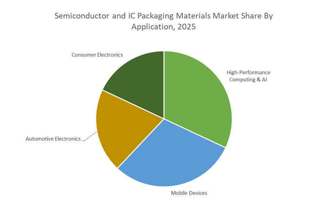
Market Share by Application: HPC & AI Lead as Chiplet Architectures and High-Bandwidth Compute Drive Unprecedented Packaging Material Demand
High-Performance Computing (HPC) and Artificial Intelligence (AI) applications dominate with a 32% share, reflecting their unparalleled need for massive data throughput, dense I/O connectivity, and optimized power-performance characteristics—requirements that conventional packaging technologies cannot meet. Modern AI accelerators, GPUs, and data center processors routinely exceed 100 billion transistors and require tens of thousands of I/O connections to interface with stacked memory (HBM), networking dies, and compute chiplets. Only advanced packaging platforms—leveraging technologies such as 2.5D interposers, 3D die stacking, CoWoS, and embedded multi-die interconnects—can provide the routing density and power delivery infrastructure necessary to support these ultra-complex architectures.
HPC and AI workloads also consume extraordinary amounts of energy, making interconnect power efficiency a core design requirement. AP materially improves the Power Performance Area Cost (PPAC) profile by shortening interconnect lengths, reducing resistance-capacitance overheads, and lowering the overall power-per-bit transferred—an essential improvement for hyperscale computing environments where thermal budgets and operational costs are tightly constrained. Additionally, the accelerating industry transition toward chiplet-based architectures relies entirely on advanced packaging to enable heterogeneous integration, allowing multiple dies—CPU, GPU, I/O, memory, and accelerators—to be assembled into a single, high-performance computing module. As AI training models scale toward trillions of parameters and HPC applications expand into exascale computing, the reliance on advanced packaging materials intensifies, solidifying HPC & AI as the fastest-growing and most influential application segment in the IC packaging ecosystem.
Country Analysis: Global IC Packaging Materials Development Hubs
Taiwan – Advanced Packaging Leadership Fueled by CoWoS®, HBM Integration, and Foundry–Materials Co-Development
Taiwan remains the global stronghold of advanced semiconductor packaging, propelled by its unmatched integration of foundry operations and cutting-edge packaging lines. As the epicenter of the High-Bandwidth Memory (HBM) packaging boom and the backbone of AI accelerator manufacturing, Taiwan—led by TSMC—continues to define the performance standards for next-generation IC packaging materials. In 2025, TSMC began transitioning from CoWoS-S (large silicon interposers) to CoWoS-L (Local Silicon Interconnect), reducing dependence on oversized interposers, enhancing overall wafer yield, and lowering integration costs for AI and HPC processors. This shift directly increases demand for high-performance dielectrics, underfill materials, and thermally conductive compounds capable of supporting increasingly dense HBM stacks.
Material suppliers remain tightly integrated into Taiwan’s innovation pipeline. Resonac Corporation, honored with the 2025 TSMC Excellent Performance Award, is a pivotal contributor to TSMC’s packaging ecosystem through its advanced encapsulation materials and in-country production of high-purity process gases. Taiwan is also shaping the future of Co-Packaged Optics (CPO), a technology that requires new families of low-loss dielectric materials, ultra-clean bonding surfaces, and thermally stable optical adhesives to support processor bandwidths up to 1.6 Tbps. Additionally, Taiwan’s TSMC-SoIC® for true 3D stacking is accelerating the adoption of TCB materials, TSV-compatible polymers, ultra-thin RDL dielectrics, and micro-bump alternatives, positioning the island as the uncontested global hub for 2.5D/3D heterogeneous integration.
United States – Hybrid Bonding, Chiplet Architecture, and CHIPS Act-Driven Packaging Material Expansion
The United States is rapidly transforming into a leading center for hybrid bonding and chiplet-based heterogeneous integration, driven by major investments from Intel, government incentives, and a growing ecosystem of advanced packaging suppliers. Intel’s Foveros Direct is at the forefront of this transition, adopting copper-to-copper hybrid bonding that eliminates traditional solder microbumps and achieves interconnect pitches below 10 micrometers. This leap requires highly specialized planarization materials, oxide bonding surfaces, wafer-level bonding layers, and ultra-low modulus dielectrics to support reliable vertical stacking.
Intel’s hybrid architecture blends Foveros (3D stacking) and EMIB (silicon bridge-based 3.5D integration), pushing demand for materials like low-CTE Epoxy Molding Compounds (EMCs) designed to mitigate thermal mismatches between silicon, organic substrates, and interconnect bridges. The CHIPS and Science Act amplifies these commercial drivers, injecting billions into new U.S. advanced packaging fabs in Arizona and Ohio. This has triggered large-scale domestic demand for BGA substrates, underfills, advanced solder pastes, non-conductive films (NCF), copper pillar plating materials, and wafer-level encapsulants. With U.S. research institutions simultaneously advancing next-generation 3D integration and heterogeneous architectures, the country is emerging as a global nucleus for high-density packaging materials and hybrid bonding innovation.
South Korea – High-Bandwidth Memory (HBM) Packaging Materials and Accelerated 3D IC Production
South Korea's dominance in memory manufacturing fuels critical innovation in packaging materials for High-Bandwidth Memory (HBM), vertical 3D stacking, and advanced interconnect processes. Samsung Electronics has established a dedicated Advanced Package Business Team and is aggressively scaling its hybrid bonding production lines to support HBM4 and beyond. HBM4—in mass deployment from 2025—requires custom dielectric films, Non-Conductive Pastes (NCP), wafer-level underfills, and ultra-stable passivation materials capable of supporting ultra-narrow microbump pitches and multi-stack DRAM assemblies with increased thermal loads.
The country’s unique combination of memory, foundry, and advanced packaging capabilities allows Samsung to tailor materials for chiplet-based logic–memory integration. This includes co-optimizing materials for thermal dissipation, warpage control, and stress mitigation. With the South Korean government allocating approximately 590 billion KRW in its 2026 strategic technology budget—including semiconductor material R&D—local suppliers are accelerating the development of low-warpage EMCs, laser-drillable substrates, and fine-pitch redistribution layer (RDL) polymers. This positions South Korea as a strategic global hub for HBM-specific packaging materials, essential to AI servers, HPC processors, and next-generation data center accelerators.
Japan – Photoresists, Advanced Films, and Critical Materials for RDL, Lithography, and Packaging Reliability
Japan remains indispensable to the global semiconductor packaging materials supply chain, thanks to its monopoly-like presence in photoresists, advanced functional films, and high-purity process chemicals. Companies such as JSR Corporation and Tokyo Ohka Kogyo (TOK) continue to supply industry-leading EUV photoresists and immersion lithography materials necessary for fabricating ultra-fine Redistribution Layers (RDLs) in Fan-Out Wafer-Level Packaging (FO-WLP). These materials are fundamental to achieving sub-micron line width/spacing (L/S) required for high-density chiplet interconnects.
Japan’s materials leadership extends further into release films, die-attach adhesives, and polyurethane resins essential for advanced substrate manufacturing and flexible printed circuit boards (FPCBs). Mitsui Chemicals plays a central role in developing heat-resistant, stress-reduced polymer films that enable next-generation FO-WLP and Panel-Level Packaging (PLP). Additionally, Resonac’s recognition by TSMC for establishing a stable, localized high-purity process gas supply chain underscores Japan’s ongoing contributions to backend semiconductor material reliability. With unparalleled precision chemical manufacturing, Japan remains the backbone of high-performance packaging materials, especially where purity, uniformity, and nanoscale process control are mission-critical.
China – Domestic OSAT Expansion, Embedded-Die Packaging, and Strategic Materials Substitution
China is accelerating its presence in the Semiconductor and IC Packaging Materials Market through aggressive investment in domestic OSAT (Outsourced Semiconductor Assembly and Test) expansion and localized material production. The National Integrated Circuit Industry Investment Fund (Big Fund) continues to inject billions into packaging technologies that reduce reliance on foreign vendors, prioritizing Embedded-Die (ED) packaging, 2.5D integration, and flip-chip technologies. China is positioning Embedded-Die as the fastest-growing segment in its packaging industry, driving demand for ultra-thin substrate materials, high-flow encapsulants, modified BT resins, and low-stress die-attach compounds tailored for ED architectures.
China’s large consumer electronics manufacturing base ensures that Flip-Chip (FC) packaging remains the highest-volume material segment, requiring extensive use of solder bumps, underfills, capillary fillers, copper pillar plating materials, and organic laminates. Domestic companies are scaling manufacturing of high-end packaging substrates and thin-film encapsulants to mitigate import risks, especially in advanced mobile, networking, and IoT devices. Meanwhile, China’s push for self-sufficiency in semiconductor materials continues to accelerate investment in process gases, dielectric films, and plating chemistries. These developments firmly position China as a rapidly maturing hub for cost-optimized, high-volume IC packaging materials, with growing strategic relevance in global supply chain realignment.
Competitive Landscape: Global Leaders Driving Advanced Semiconductor Packaging Materials
The competitive landscape is defined by companies specializing in substrate films, molding compounds, photoresists, thermal interface materials, epoxy systems, and dielectric materials. Market leadership is increasingly tied to innovation in CTE control, dielectric properties, thermal performance, sustainability, and high-density interconnect (HDI) capability.
Ajinomoto leads the global market for ABF (Ajinomoto Build-Up Film), the insulating material of choice for CPUs, GPUs, and AI accelerators since 1999. Derived from the company’s expertise in amino-acid fine chemistry, ABF exhibits low thermal expansion, excellent rigidity, and superior dielectric stability for GHz-level signal transmission. A key competitive advantage lies in ABF’s laser-friendly surface, enabling microvias and ultra-fine circuit formation essential for HDI substrates used in 2.5D/3D packages. Ajinomoto continues to evolve ABF compositions to support chiplet-based designs, HBM integration, and ultra-high-density routing, aligning with advanced manufacturing for AI workloads and next-generation server processors.
Fujifilm leverages its extensive chemistry portfolio to offer end-to-end materials spanning EUV resists, ArF resists, CMP slurries, polyimides, and packaging chemicals. The company’s planned investment exceeding 100 billion JPY (FY2025–2026) strengthens its development pipeline for high-performance materials addressing 2 nm and beyond. Fujifilm also leads the market in AI-enabled quality control, incorporating image recognition systems to detect fine particles and contamination during material production. Its expanding manufacturing capacity and rapid innovation cycles reinforce its position as a critical supplier for lithography and next-generation packaging.
Sumitomo Bakelite remains a top supplier of Epoxy Molding Compounds (EMCs) and Copper-Clad Laminates (CCL) used across semiconductor packaging, automotive electronics, and 5G infrastructure. Its LαZR® interposer material offers a high modulus and low CTE profile, directly addressing package warpage and thin substrate reliability issues. Sumitomo’s strategic focus on mobility (ADAS), 5G communication, and ultra-low dielectric materials positions it at the intersection of high-frequency, high-power semiconductor applications. The commercialization of a biomass-derived phenolic resin (June 2025) underscores its leadership in sustainable material innovation.
Formerly Hitachi Chemical, Resonac continues to lead in EMC development, supplying materials for encapsulation across mobile devices, automotive modules, and advanced packaging platforms. Its heavy investment in Green EMCs reduces VOC emissions and aligns with the sustainability requirements of major semiconductor manufacturers. Resonac’s portfolio includes thermally conductive, high-modulus EMCs optimized for System-in-Package (SiP), FOWLP, and high-temperature automotive electronics, where reliability under thermal stress is critical. The company is strategically adjusting formulations to meet the evolving needs of multi-die, 3D stacked and heterogeneous packages.
Shin-Etsu’s portfolio spans silicone encapsulants, gel compounds, liquid encapsulants, and die-attach pastes, all optimized for reliability under thermal and environmental stress. The company differentiates itself through advanced stress-reduction and moisture-control silicone technologies, particularly in its SMC series liquid encapsulants launched in August 2025. These materials are engineered for large die underfills and organic substrates, mitigating warpage and cracking in high-power semiconductor packages. Shin-Etsu continues to expand its presence in automotive, EV power electronics, and wearable devices, sectors where thermal cycling resilience is non-negotiable.
Semiconductor and IC Packaging Materials Market Report Scope
Semiconductor and IC Packaging Materials Market
|
Parameter
|
Details
|
|
Market Size (2025)
|
$52.3 Billion
|
|
Market Size (2035)
|
$120.4 Billion
|
|
Market Growth Rate
|
8.7%
|
|
Segments
|
By Material Type (Substrates, Bonding Materials, Encapsulation Materials, Dielectric Materials), By Packaging Type (Advanced Packaging, Conventional Packaging), By Application (High-Performance Computing & AI, Mobile Devices, Automotive Electronics, Consumer Electronics), By Function (Structural/Support, Interconnect, Protection/Encapsulation, Insulation/Signal Integrity), By Process Step (Wafer Level Packaging Materials, Die Attach Materials, Wire Bonding Materials, Molding & Curing Materials)
|
|
Study Period
|
2019- 2024 and 2025-2034
|
|
Units
|
Revenue (USD)
|
|
Qualitative Analysis
|
Porter’s Five Forces, SWOT Profile, Market Share, Scenario Forecasts, Market Ecosystem, Company Ranking, Market Dynamics, Industry Benchmarking
|
|
Companies
|
Resonac Corporation, Tanaka Holdings Co. Ltd., Sumitomo Bakelite Co. Ltd., Ajinomoto Co. Inc., Intel Corporation, DuPont de Nemours Inc., JSR Corporation, Henkel AG & Co. KGaA, Shin-Etsu Chemical Co. Ltd., Kyocera Corporation, Dow Inc., BASF SE
|
|
Countries
|
US, Canada, Mexico, Germany, France, Spain, Italy, UK, Russia, China, India, Japan, South Korea, Australia, South East Asia, Brazil, Argentina, Middle East, Africa
|
Semiconductor and IC Packaging Materials Market Segmentation
By Material Type
- Substrates (BT Resin, Glass Core Substrates, Ceramics, Epoxy-based Laminates)
- Bonding Materials (Solder Balls, Copper Wire, Gold Wire, Non-Conductive Paste, Hybrid Bonding Adhesives)
- Encapsulation Materials (Epoxy Molding Compound, Liquid Encapsulants)
- Dielectric Materials (Porous Low-k Films, Thin Film Resins)
By Packaging Type
- Advanced Packaging (2.5D/3D ICs, Fan-Out Wafer Level Packaging, System-in-Package, Chiplet Integration)
- Conventional Packaging (BGA, QFN, DIP, QFP, Leadframe-based)
By Application
- High-Performance Computing & AI
- Mobile Devices
- Automotive Electronics
- Consumer Electronics
By Function
- Structural / Support
- Interconnect
- Protection / Encapsulation
- Insulation / Signal Integrity
By Process Step
- Wafer Level Packaging Materials
- Die Attach Materials
- Wire Bonding Materials
- Molding and Curing Materials
By Region
- North America (United States, Canada, Mexico)
- Europe (Germany, France, United Kingdom, Spain, Italy, Rest of Europe)
- Asia Pacific (China, India, Japan, South Korea, Australia, Rest of APAC)
- South and Central America (Brazil, Argentina, Rest of SCA)
- Middle East and Africa (Saudi Arabia, UAE, South Africa, Rest of Middle East, Rest of Africa)
Top Companies: Key Semiconductor and IC Packaging Materials Manufacturers
- Resonac Corporation (Showa Denko/Hitachi Chemical)
- Tanaka Holdings Co., Ltd.
- Sumitomo Bakelite Co., Ltd.
- Ajinomoto Co., Inc.
- Intel Corporation
- DuPont de Nemours, Inc.
- JSR Corporation
- Henkel AG & Co. KGaA
- Shin-Etsu Chemical Co., Ltd.
- Kyocera Corporation
- Dow Inc.
- BASF SE
*- List not Exhaustive
