
The semiconductor manufacturing market is in the midst of rapid transformation, driven by massive global investments, next-generation production technologies, and regional capacity expansions. In May 2025, TSMC unveiled plans for new advanced-node fabrication plants, investing around USD 28 billion in cutting-edge chip fabs across the U.S. (Arizona), Taiwan, and Japan. This aggressive expansion reinforces TSMC’s role at the forefront of leading-edge chip production worldwide. At the same time, both Samsung and Intel are ramping up their global footprints Samsung with significant new foundry investments in the U.S. (such as Taylor, Texas) focused on AI and high-performance computing chips, and Intel with the September 2024 inauguration of Fab 34 in Ireland, designed for high-volume Intel 4 process technology. GlobalFoundries is also doubling its capacity for mature and specialty chip production with the ongoing expansion of Fab 8 in Malta, New York, while SK Hynix is establishing advanced packaging plants in the U.S., highlighting the rising importance of high-bandwidth memory (HBM) for AI and data center applications.
Groundbreaking equipment innovations are further propelling the semiconductor manufacturing industry into a new era of miniaturization and complexity. Applied Materials introduced state-of-the-art extreme ultraviolet (EUV) lithography systems in January 2025, targeting the sub-3nm technology nodes required for the smallest and most powerful chips. ASML launched its next-generation EUV manufacturing equipment featuring AI-driven process optimization, offering chipmakers unprecedented control over yield and efficiency. Equipment suppliers such as Lam Research are rolling out advanced etch and deposition systems, optimized for 3nm and 2nm nodes, enabling the fabrication of complex 3D transistor architectures. Tokyo Electron (TEL) is expanding its R&D and production of coater/developer and plasma etch systems, which are critical in the photolithography process and essential for next-gen semiconductor devices.
Quality control, yield management, and process monitoring have become essential pillars of semiconductor production as geometries shrink and device complexity rises. KLA Corporation is responding to these challenges by continuously introducing new metrology and inspection tools, allowing manufacturers to detect minuscule defects and ensure the highest possible quality at every stage of production. The ongoing expansion and integration of advanced manufacturing technologies and process control solutions are empowering chipmakers to keep pace with soaring global demand and the technological leaps required for artificial intelligence, automotive electronics, and next-generation computing. Collectively, these recent developments are propelling the semiconductor manufacturing market to new heights, reinforcing its critical role at the heart of the digital economy.
The semiconductor manufacturing industry is embracing a transformative trend with the integration of Quantum Machine Learning (QML) for advanced wafer defect prediction and real-time correction. Unlike conventional AI-based models, QML harnesses the power of quantum computing to process vast and complex datasets at unprecedented speeds, delivering superior accuracy in identifying defects at the most advanced technology nodes, including sub-3nm processes. This leap in predictive precision is critical for optimizing yield rates, reducing manufacturing errors, and lowering overall production costs in high-volume chip fabrication.
Beyond prediction, QML-driven real-time process correction is becoming a game changer for accelerating yield ramp-up in next-generation semiconductor architectures such as Gate-All-Around FET (GAAFET) transistors. By enabling near-instantaneous adjustments during lithography and etching steps, QML ensures tighter process control and consistency, reducing cycle times and improving throughput. This capability is especially valuable in an industry where rapid node migration and high manufacturing efficiency directly influence profitability. As leading chipmakers and foundries adopt QML-based platforms, the technology is set to redefine defect management, positioning QML as a cornerstone of next-gen semiconductor manufacturing.
A major cost-saving opportunity in semiconductor manufacturing lies in recycling and reconditioning EUV (Extreme Ultraviolet) pellicles critical components that protect masks during EUV lithography. Currently, single-use pellicles constitute a significant operational expense for fabs, particularly as demand for advanced lithography scales with nodes shrinking toward 2nm and beyond. Recycling initiatives, including chemical reconditioning and pellicle refurbishment, have the potential to extend component lifespan substantially, translating into millions in annual savings per fab.
Leading semiconductor equipment companies are actively developing innovative business models such as pellicle leasing and refurbishment programs to mitigate these escalating costs. These approaches not only reduce capital expenditures for chipmakers but also enhance sustainability by minimizing material waste in highly resource-intensive manufacturing environments. As the industry pushes deeper into next-generation lithography, cost optimization through pellicle recycling will play a pivotal role in maintaining competitiveness and enabling broader adoption of EUV technology across the semiconductor ecosystem.
ASML: Dominance in EUV Lithography and Next-Generation Patterning Solutions
ASML continues to shape the future of the semiconductor manufacturing market with its unrivaled dominance in EUV lithography systems. As the exclusive provider of EUV technology, ASML’s platforms enable advanced chip nodes such as 3nm, 2nm, and the anticipated sub-2nm processes that power everything from AI data centers to next-gen smartphones. The introduction of its High-NA EUV lithography systems (EXE platform) marks a pivotal advancement, allowing even smaller feature sizes and driving Moore’s Law forward into the second half of the 2020s. In 2025, ASML’s delivery of its first High-NA EUV system to customers signaled the transition from research to process development for future high-volume manufacturing, establishing its critical position in advanced logic and memory chip production. The company’s ongoing investments in computational lithography software, metrology, and inspection tools optimize yield and process performance, catering to the increasing complexity of patterning at atomic scales. ASML’s focus on sustainability is evident in its efforts to expand refurbished equipment offerings, support circular manufacturing, and reduce the environmental footprint of semiconductor fabrication. Additionally, ASML is preparing to enter the advanced packaging market with new fast i-line systems, targeting the booming demand for chiplet-based architectures and 3D integration. Despite facing geopolitical headwinds and export restrictions particularly with China ASML maintains a robust order backlog, reflecting strong global demand for its indispensable lithography solutions and further reinforcing its central role in the semiconductor manufacturing equipment market.
Applied Materials stands as a global powerhouse in semiconductor materials engineering and wafer fabrication equipment, supplying deposition, etch, CMP (chemical mechanical planarization), ion implantation, and metrology systems across the entire semiconductor manufacturing value chain. The company is renowned for pioneering integrated materials solutions, which combine multiple process steps and in-situ metrology within a single system to improve chip performance, yield, and time-to-market. In response to the growing complexity of AI chips and advanced packaging, Applied Materials is expanding its global manufacturing capacity in the US and Singapore, ensuring it can meet the surge in customer demand driven by digitalization and government-backed localization efforts. With its PPACt (Power, Performance, Area, Cost, and Time-to-market) playbook, Applied Materials is at the forefront of developing innovative materials, such as new dielectrics and barrier films, to enable faster, smaller, and more energy-efficient devices. Recent initiatives include major investments in R&D facilities and collaboration with leading foundries to accelerate the commercialization of next-generation transistors and advanced memory. The company’s strategic push into India’s semiconductor ecosystem underscores its commitment to supporting emerging manufacturing hubs and fostering supply chain resilience. Applied Materials’ robust suite of process control, inspection, and analytics software further supports fabs in achieving atomic-level precision and continuous yield improvement, making it a vital player in the ongoing evolution of the semiconductor manufacturing equipment market.
Tokyo Electron (TEL) is a top-tier supplier of semiconductor production equipment, providing comprehensive process solutions that span photolithography coater/developers, plasma etchers, deposition systems, cleaning equipment, and wafer probers. TEL’s reputation for reliability, precision, and innovation has made its equipment foundational in advanced wafer fabrication for leading foundries and integrated device manufacturers worldwide. The company’s strategic focus on R&D is reflected in its partnerships with research organizations like imec, accelerating the development of beyond-2nm technology nodes. Recent product launches include the LEXIA™-EX PVD sputtering system and the Acrevia™ gas cluster beam system, both designed to enable ultra-fine patterning essential for EUV lithography and high-density 3D NAND flash production. TEL’s commitment to sustainability is demonstrated by its science-based net zero greenhouse gas emission targets for 2040 and its ongoing initiatives to enhance energy and resource efficiency across its product portfolio. The company has also received industry recognition for its digital transformation efforts and customer service excellence. As the semiconductor market shifts toward more complex, multi-patterning, and heterogeneous integration, TEL’s versatile equipment solutions and process expertise remain integral to supporting high-volume manufacturing at advanced and legacy nodes alike.
Lam Research is a critical enabler in the wafer fabrication equipment sector, specializing in advanced plasma etch, thin film deposition, wafer cleaning, and photoresist strip solutions. Lam’s systems are vital for creating the intricate, high-aspect-ratio features required in leading-edge logic, memory, and 3D NAND devices. The company is pioneering the adoption of AI and virtual fabrication platforms through its Semiverse® Solutions, which leverage machine learning for process optimization, faster new product introduction, and enhanced yield management. Lam Research is also heavily invested in supporting the growth of advanced packaging technologies, which are central to next-generation chiplet architectures and heterogeneous integration. Sustainability is a core pillar of Lam’s strategy, with ongoing efforts to reduce the environmental impact of its manufacturing processes and to help customers achieve their own net zero goals. Global expansion and customer partnerships, particularly in markets like India and Southeast Asia, further cement Lam Research’s role as a key technology provider in both established and emerging semiconductor manufacturing ecosystems. As the complexity of device architectures increases, Lam’s advanced process equipment and data-driven solutions ensure manufacturers can continue to scale performance while controlling cost and maintaining reliability.
KLA is the market leader in process control, inspection, and metrology systems for semiconductor manufacturing, playing a pivotal role in helping fabs achieve high yield, reliability, and efficiency at the most advanced technology nodes. The company’s defect inspection tools, broadband plasma systems, and high-precision metrology solutions are used throughout the wafer, mask, and packaging process, providing real-time data and analytics to optimize manufacturing outcomes. KLA’s recent $138 million investment in a new R&D and manufacturing facility in Newport, Wales, has significantly expanded its capabilities in advanced packaging and wafer processing, including plasma etch, PVD, and PECVD for MEMS, power semiconductors, and photonics. With AI-driven solutions integrated into its hardware and software platforms, KLA accelerates innovation by enabling faster defect detection, process tuning, and yield improvement capabilities that are indispensable for high-volume, high-complexity chip production. The company’s expanding portfolio in advanced packaging underscores the growing importance of 2.5D and 3D integration in the semiconductor roadmap. KLA’s close customer collaboration and continuous measurement innovation make it an essential partner for fabs seeking to navigate the challenges of atomic-scale manufacturing and maintain competitiveness in a rapidly advancing industry.
Front-end wafer fabrication dominates with the largest market share of 60.2% in 2025, reflecting the capital-intensive nature of EUV lithography, thin-film deposition, and etching steps in sub-5nm and 3nm nodes. Back-end processes, including assembly, testing, and packaging, remain essential for yield optimization and final product reliability, benefiting from strong outsourcing trends to OSATs like ASE and Amkor. Advanced Packaging is the fastest-growing segment, projected at a CAGR of 10.1%, driven by 3D IC stacking, chiplet-based architectures, and heterogeneous integration for AI/ML workloads and high-performance computing, as Moore’s Law slows down.
.png)
Logic processors hold the largest share at 39.6% in 2025, fueled by soaring demand for CPUs, GPUs, and AI accelerators powering 5G infrastructure, data centers, and edge computing devices. Memory (DRAM and NAND) remains a crucial application but faces cyclical pricing trends that temper its overall growth. Sensors and MEMS devices, vital for automotive and IoT ecosystems, grow steadily with smart mobility adoption. Power semiconductors represent the fastest-growing segment at a CAGR of 9.2%, supported by the rapid transition to electric vehicles, renewable energy systems, and wide-bandgap materials like silicon carbide (SiC) and gallium nitride (GaN) for high-efficiency power conversion.
The United States is aggressively reclaiming its position as a semiconductor powerhouse, propelled by unprecedented government support through the CHIPS and Science Act. As of mid-2025, federal funds are actively reshaping the domestic landscape, with Micron Technology securing $6.2 billion for new memory fabs in Idaho and New York, plus additional expansion in Virginia. This funding is part of a broader, $200 billion+ plan to cement U.S. leadership in memory, logic, and advanced packaging, with a key milestone being the localization of High Bandwidth Memory (HBM) production. Simultaneously, Intel is ramping up its Arizona “Intel 18A” line, which achieved production status in July 2025. Although Intel slowed some overseas projects, its U.S. fabs are set to anchor next-generation process nodes critical for AI, defense, and cloud markets.
Major global foundries are deepening their U.S. footprint, underscored by TSMC’s Arizona facility beginning 4nm chip output at the end of 2024, serving giants like Apple and NVIDIA, with a second fab for 3nm chips already under accelerated construction. Samsung is finalizing its $44 billion Texas plant upgrade, aiming for 2nm output by 2026, supported by $6.6 billion in CHIPS Act funds. These projects not only reinforce the U.S. supply chain but signal a major shift toward regionalization in semiconductor value creation, emphasizing advanced logic, memory, and the development of AI-optimized hardware.
Taiwan maintains its position as the world’s semiconductor linchpin, led by TSMC’s unmatched dominance in foundry services and advanced packaging. While TSMC’s Arizona and Kumamoto (Japan) fabs draw global attention, its most advanced R&D and back-end processes such as CoWoS and SoIC will remain largely in Taiwan for the foreseeable future. The island’s fabs are moving rapidly toward the A16 and N2 process nodes, reinforcing its lead in high-performance logic chips.
Despite rising geopolitical risks and government-driven incentives to diversify, Taiwan’s advanced manufacturing and packaging ecosystem remains irreplaceable, especially for chips that power AI, smartphones, and automotive markets. Upcoming milestones, such as the opening of TSMC’s third and fourth local mega-fabs, will further cement Taiwan’s strategic importance. The ongoing reliance on domestic R&D and core manufacturing ensures Taiwan’s critical role in both global supply chains and technology innovation.
South Korea’s semiconductor sector is intensifying its pursuit of advanced process nodes, with Samsung Foundry actively investing in 2nm technology both domestically and in the U.S., despite the latter’s project delays due to technology upgrades. Meanwhile, SK Hynix is riding the global HBM wave, projecting a 75% CapEx jump in 2025 as demand for AI memory surges (with HBM demand up 200% in 2024 and forecasted to grow another 70% in 2025). This arms race is fueled by insatiable demand for DRAM and NAND in data center and AI workloads.
Government incentives, coordinated R&D, and ecosystem partnerships are cornerstones of Korea’s strategy, enabling both Samsung and SK Hynix to remain fiercely competitive on cost, technology, and scale. South Korea’s focused approach is set to keep it at the forefront of advanced memory and foundry manufacturing in the AI era.
Japan’s semiconductor revival is being realized through heavy government funding and cutting-edge collaborative ventures. Rapidus Corp., backed by $1.3 billion in new 2025 funding atop an earlier $6.5+ billion commitment, is targeting mass production of 2nm chips by 2027 at its Hokkaido plant. The December 2024 installation of ASML’s EUV lithography tool marks a historic milestone, restoring Japan’s advanced manufacturing capability.
Strategic alliances with IBM (for 2nm GAA process) and Cadence (for AI-optimized design flows) underscore a modern approach to rapid catch-up and leapfrog innovation. Japan’s domestic supply chain is also being bolstered by a renewed focus on material science, equipment, and R&D talent, positioning the nation as a rising competitor in sub-5nm chip production for the next decade.
China is pushing hard toward semiconductor independence amid global supply chain turbulence and export controls. By 2025, the country’s self-sufficiency rate in chipmaking equipment is expected to reach 50%, up from 13.6% in 2024, with notable progress in etching, cleaning, and photoresist technologies. “The Big Fund” (China’s national chip fund) continues to pour capital into HBM, mature-node chips, and domestic design IP particularly RISC-V, seen as a strategic alternative to ARM.
China’s prowess in mature-node chips (28nm+) is already reshaping markets for electric vehicles, IoT, and solar, while advanced node ambitions are being realized through persistent investment, technology transfers, and policy support. As geopolitical decoupling continues, China’s strategy of scaling mature process nodes and nurturing homegrown IP will make it a formidable force in specific verticals, even as it lags in extreme leading-edge logic.
Germany is the undisputed hub of European semiconductor manufacturing, spearheaded by major investments in Dresden. Infineon’s €5 billion Smart Power Fab backed by €920 million in federal support will debut the world’s first flexible line for processing multiple technologies on a single 300mm wafer. Simultaneously, the European Semiconductor Manufacturing Company (ESMC) a joint venture between TSMC (70%), Bosch, NXP, and Infineon (10% each) has commenced building its new foundry with substantial state and EU funding.
These projects are central to the European Chips Act’s vision of securing 20% of global semiconductor output for the EU by 2030. Germany’s focus on power semiconductors, automotive chips, and next-gen logic underscores the country’s role as a continental manufacturing and R&D anchor.
India’s semiconductor ecosystem is shifting rapidly from policy groundwork to execution. By July 2025, six major manufacturing proposals have secured government approval and funding. Micron’s $1.5 billion ATMP (Assembly, Testing, Marking, and Packaging) facility in Gujarat and the new HCL-Foxconn fab are headline examples. India is intentionally building expertise in analog, power, and OSAT, with a phased approach to full-stack manufacturing.
Government programs are now deepening the domestic supply chain scaling up tooling, automation, and high-precision equipment while Indian companies are acquiring global IP and R&D assets. The nation’s focus on capability building rather than chasing advanced logic nodes from the outset is a pragmatic play that could eventually position India as a major OSAT and specialty chip hub in the region.
France’s role in European semiconductor manufacturing is being defined by STMicroelectronics’ digital wafer capacity expansion in Crolles. With weekly output set to rise to 14,000 wafers (with further potential), the facility’s transformation will also support advanced packaging and wafer-level testing, crucial for Europe’s digital infrastructure. ST’s heavy investment in R&D at 16% of revenue demonstrates the company’s long-term commitment to innovation and high-value chip technologies.
Strategic collaborations with TSMC and Samsung help STMicroelectronics maintain competitiveness in advanced nodes, including FinFET and FD-SOI, enhancing both domestic French and broader European capabilities in logic, power, and automotive semiconductors.
|
Parameter |
Details |
|
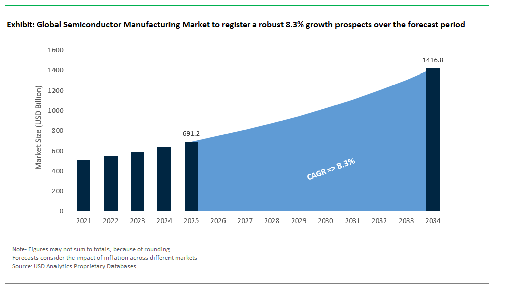
Market Size (2025) |
$691.2 Billion |
|
Market Size (2034) |
$1416.6 Billion |
|
Market Growth Rate |
8.3% |
|
Segments |
By Process Type (Front-end (Wafer fabrication), Back-end (Assembly, testing, packaging), Advanced packaging (3D IC, chiplets)), By Technology Node (Up to 7nm, 16nm, 28nm), By Business Model (Integrated Device Manufacturers (IDMs), Fabless Semiconductor Companies, Foundries (Pure-Play Foundries), Outsourced Semiconductor Assembly and Test (OSAT) Companies), By Application (Logic processors, Memory (DRAM, NAND), Power semiconductors, Sensors/MEMS), By Material (Silicon wafers, Compound semiconductors (GaN, SiC), Photoresists/gases) |
|
Study Period |
2019- 2024 and 2025-2034 |
|
Units |
Revenue (USD) |
|
Qualitative Analysis |
Porter’s Five Forces, SWOT Profile, Market Share, Scenario Forecasts, Market Ecosystem, Company Ranking, Market Dynamics, Industry Benchmarking |
|
Companies |
Taiwan Semiconductor Manufacturing Company (TSMC) Ltd., Samsung Electronics Co. Ltd., Intel Corporation, SK Hynix Inc., Micron Technology Inc., Qualcomm Incorporated, NVIDIA Corporation, Broadcom Inc., Advanced Micro Devices (AMD) Inc., Texas Instruments Inc., ASML Holding N.V. (Equipment), Applied Materials Inc. (Equipment), Lam Research Corporation (Equipment), Tokyo Electron Ltd. (Equipment), KLA Corporation (Equipment), Synopsys Inc. (EDA Software), Cadence Design Systems, Inc. (EDA Software), NXP Semiconductors N.V., Infineon Technologies AG, STMicroelectronics N.V., Analog Devices Inc., onsemi (ON Semiconductor Corp.), Renesas Electronics Corporation, GlobalFoundries Inc., United Microelectronics Corporation (UMC), Semiconductor Manufacturing International Corporation (SMIC) |
|
Countries |
US, Canada, Mexico, Germany, France, Spain, Italy, UK, Russia, China, India, Japan, South Korea, Australia, South East Asia, Brazil, Argentina, Middle East, Africa |
* List Not Exhaustive
The Semiconductor Manufacturing Market report by USDAnalytics offers an in-depth analysis of global market sizing, CAGR, and value projections, highlighting recent developments such as TSMC’s $28 billion advanced-node fab expansion, Samsung and Intel’s global investments, and ASML’s next-generation EUV lithography breakthroughs. The study provides in-depth market sizing, CAGR, and value projections, placing recent developments such as quantum machine learning for defect prediction, AI-driven process optimization, EUV pellicle recycling, and regional government incentives at the center of industry transformation.
Market segmentation covers process type (front-end wafer fabrication, back-end assembly/testing/packaging, advanced packaging), technology node (up to 7nm, 16nm, 28nm), business model (IDMs, foundries, fabless, OSAT), application (logic processors, memory, power semiconductors, sensors/MEMS), and materials (silicon wafers, compound semiconductors, photoresists/gases). The report includes comprehensive company profiles and recent advancements from TSMC, Samsung, Intel, SK Hynix, ASML, Applied Materials, Lam Research, Tokyo Electron, KLA, and key OSAT and EDA software leaders.
The analysis covers historical data from 2021–2024 and forecasts through 2025–2034. Geographic coverage includes North America (US, Canada, Mexico), Europe (Germany, UK, France, Italy, Russia, Rest of Europe), Asia Pacific (China, India, Japan, South Korea, Australia, Southeast Asia, Rest of Asia), South America, and Middle East & Africa.
The report delivers actionable insights for industry professionals, investors, equipment suppliers, and policymakers, with detailed coverage of market dynamics, technology roadmaps, innovation, competitive landscape, global supply chain, and future growth opportunities in the semiconductor manufacturing sector.
Table of Contents: Semiconductor Manufacturing Market
1. Executive Summary
2. Semiconductor Manufacturing Market Landscape & Outlook (2025–2034)
3. Breakthrough Innovations in the Semiconductor Manufacturing Market
4. Competitive Landscape: Semiconductor Manufacturing Equipment Market
5. Market Share and Segmentation Insights: Semiconductor Manufacturing Market
6. Country Analysis and Outlook of Semiconductor Manufacturing Market
7. Semiconductor Manufacturing Market Size Outlook by Region (2025-2034)
8. Company Profiles: Leading Players in Semiconductor Manufacturing Market
9. Methodology
10. Appendix
The global semiconductor manufacturing market is valued at $691.2 billion in 2025 and projected to grow at a CAGR of 8.3%, reaching $1,416.6 billion by 2034.
Key trends include quantum machine learning for defect prediction, EUV pellicle recycling, advanced packaging (3D IC, chiplets), AI-powered yield management, and rapid technology node migration toward 2nm and below.
Front-end wafer fabrication holds the largest market share due to capital intensity and technology advancement, while logic processors lead by application, powering AI, 5G, and data center growth.
The U.S., Taiwan, South Korea, Japan, China, and Germany are the primary drivers, each investing heavily in advanced fabs, local supply chains, and regional technology leadership.
Major companies include TSMC, Samsung, Intel, SK Hynix, Micron, Qualcomm, NVIDIA, Broadcom, AMD, ASML, Applied Materials, Lam Research, Tokyo Electron, KLA, and others.