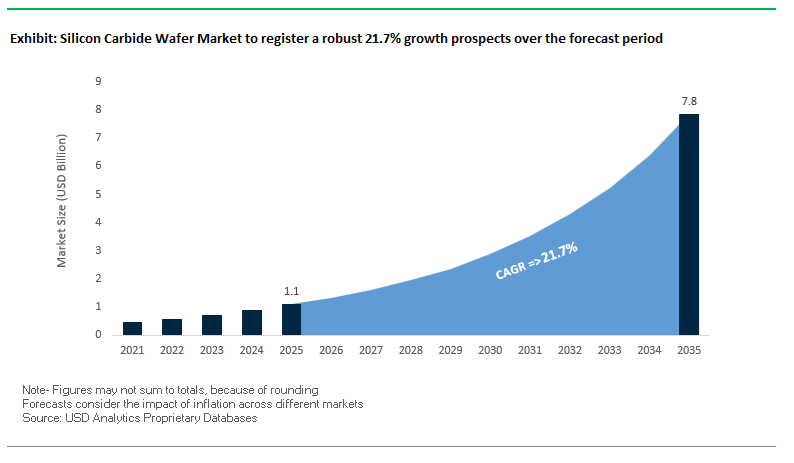
The Silicon Carbide Wafer Market, valued at USD 1.1 billion in 2025, is projected to reach USD 7.8 billion by 2035, growing at an exceptional CAGR of 21.7%. Demand for SiC wafers continues to intensify as EV power electronics, renewable energy inverters, industrial drives, and AI/hyperscale data centers transition toward wide bandgap (WBG) devices that require low-defect, high-uniformity substrates.
The SiC wafer market experienced substantial structural acceleration from 2024 to 2026, defined by aggressive capacity expansions, technological scaling, and next-generation device launches. A pivotal milestone occurred in December 2025, when Coherent Corp. announced the expansion of its SiC substrate development from 200 mm to 300 mm wafers, establishing a long-term scaling roadmap that positions the company at the forefront of substrate innovation. The move aligns with broader industry efforts to secure multi-decade WBG leadership as EVs, clean energy, and industrial power systems drive exponential SiC demand.
The global manufacturing environment, however, continues to experience volatility. According to a September 2025 SEMI Report, equipment spending on 200 mm SiC fabs will decline 12% to US$6.3 billion in 2025, followed by a modest recovery to US$6.7 billion in 2026, reflecting a temporary recalibration in capital deployment despite strong long-term growth. Meanwhile, significant capacity expansion is underway in Asia: in August 2025, TanKeBlue Semiconductor began constructing its Phase II SiC wafer expansion in Jiangsu, China, increasing annual output by 160,000 wafers to reach 230,000 wafers by August 2026, bolstering regional supply resilience.
Device-side market signals also intensified wafer demand. In May 2025, Nexperia launched a new family of SiC MOSFETs with RDS(on) values as low as 30 mΩ, driving strong wafer consumption—especially for high-performance 6-inch and early 8-inch production lines. In February 2025, Infineon Technologies AG began commercial release of its first 200 mm SiC power devices, marking the formal beginning of the 8-inch commercial transition among leading integrated device manufacturers (IDMs). Earlier in January 2025, Wolfspeed introduced its Gen 4 SiC MOSFET platform, a device architecture enabled by advanced wafer quality and epitaxy improvements.
Supporting technologies also advanced. In December 2024, X-FAB launched XSICM03, its next-generation XbloX SiC process platform featuring reduced cell pitch and enhanced die-per-wafer yield. Complementing the, Vishay’s June 2024 introduction of 16 new 1200 V Gen 3 SiC Schottky diodes sustained strong demand for high-voltage substrates, reinforcing the long-term supply chain requirements for defect-free, uniform SiC wafers.
Market buyers increasingly scrutinize wafer metrics including epitaxial defect density, diameter scalability, wafer yield, flatness, micropipe density, and thermal conductivity.
The technical parameters below highlight the economic and performance advantages driving global SiC wafer demand—specifically in fast-charging EV platforms, high-voltage industrial systems, and PV/ESS applications. The ongoing shift from 150 mm (6-inch) to 200 mm (8-inch) wafers represents the most significant transformation in the SiC supply chain, widening chip output per wafer and drastically improving device cost structure. Additionally, emerging R&D efforts in 300 mm (12-inch) substrates signal long-term scalability pathways that could bring SiC closer to silicon-level cost competitiveness.
- 8-inch scaling sharply reduces device cost: Transitioning to 200 mm SiC wafers reduces wafer cost by 30–40%, driven by higher die counts and better economies of scale.
- Epitaxy quality reaches near-perfect levels: Top suppliers report >99% defect-free epitaxial wafer area, enabling high reliability for high-voltage SiC MOSFETs and next-generation traction inverters.
- Market transition is accelerating: By 2024, 32 companies globally were already prototyping or qualifying 200 mm wafers, confirming industry-wide migration away from 150 mm standards.
- Wafer affordability is improving: A 17% price drop in 6-inch SiC wafers (2022–2024) signals stabilizing supply and maturing manufacturing efficiency.
- Long-term roadmap confirmed: Top-tier suppliers began expanding into 300 mm SiC R&D in Dec 2025, establishing the foundation for future scaling.
200mm Scaling, Vertical Integration of Epitaxy, Semi-Insulating SiC Innovation, and Wafer Reclamation Define the Future of the Silicon Carbide (SiC) Wafer Market
Trend 1: Aggressive Industry Transition to 200mm SiC Wafers Driven by Micropipe Reduction and Defect Control
The shift from 150mm to 200mm SiC wafers is the most consequential scaling event in the SiC wafer industry to date, unlocking dramatic cost reductions, expanded die-per-wafer counts, and improved competitiveness for high-volume power semiconductor applications. However, the transition hinges on success in reducing crystalline defects that historically limited SiC scalability.
Key technical advancements shaping market adoption include:
- Micropipe density breakthrough: Modern 200mm wafer prototypes have achieved MPD levels as low as 0.36/cm², a milestone that meets the threshold for high-yield power device fabrication and signals maturity in PVT crystal growth at larger diameters.
- 25% increase in crystal growth throughput: Optimized PVT furnace configurations for 200mm wafers have boosted mass deposition rates by 25%, directly improving boule production economics and lowering the effective cost per wafer.
- Resistivity uniformity retention across larger wafers: Despite expanded surface area and accelerated growth rates, 200mm SiC wafers maintain resistivity uniformity matching 150mm wafers, enabling consistent MOSFET and diode device performance across the wafer.
- Usable area ≥ 90% for Prime Grade wafers: To qualify for EV traction inverter and industrial inverter applications, manufacturers target usable area ≥ 90% and MPD ≤ 5/cm², benchmarks required for automotive OEM adoption and large-scale device yield.
This shift to 200mm Prime Grade SiC wafers sets the foundation for cost-competitive SiC power electronics that can scale into mass-market automotive, industrial, and energy applications.
Trend 2: Device Makers Accelerate Vertical Integration of Epitaxial Growth to Secure Supply and Optimize Device Performance
Epitaxy is one of the most quality-critical steps in SiC device manufacturing, directly determining device breakdown voltage, channel mobility, and threshold stability. As a result, global IDMs are rapidly internalizing epitaxial growth and substrate sourcing.
Market-defining developments include:
- Creation of fully integrated SiC campuses: STMicroelectronics is building a vertically integrated SiC campus in Italy, consolidating substrate development, epitaxial growth, and 200mm wafer processing under one facility, supported by government funding.
- Strategic internal sourcing targets: A leading IDM aims for 40% internal substrate sourcing by 2024, ensuring epi-wafer availability and reducing dependency on merchant wafer suppliers during the 200mm scaling phase.
- 15,000 wafers/week mass-production readiness: New 200mm SiC fabs in Europe are engineered for 15,000 wafers/week capacity, aligning substrate, epitaxy, and device manufacturing in a synchronized production environment.
- Customization of epi-layer properties: Vertical integration allows IDMs to tune epitaxial thickness, doping concentration, and interface defect density for 600–1200V MOSFETs-an essential voltage class expected to exceed 50 million units annually by 2025.
This consolidation dramatically improves supply assurance, reduces process variation, and accelerates optimization cycles for next-generation SiC MOSFETs and Schottky diodes.
Opportunity 1: Growing Demand for Semi-Insulating (SI) SiC Wafers for RF, Microwave, and Quantum Computing Applications
The rise of 5G/6G networks, high-power RF systems, quantum technologies, and aerospace electronics is generating exceptional demand for semi-insulating SiC substrates with extremely high resistivity and minimal crystalline defects.
Key performance enablers include:
- Ultra-high resistivity benchmark: High-Purity Semi-Insulating SiC exhibits resistivity >1×10¹² Ω·cm, necessary for isolating high-frequency signals and preventing parasitic conduction in RF power amplifiers.
- Near-zero defect targets: Research demonstrations show 6-inch SI SiC wafers with only two micropipes, validating the feasibility of ultra-low-defect substrates for next-generation RF and quantum devices.
- Preferred substrate for GaN RF devices: GaN-on-SiC remains the gold standard for high-power RF electronics due to superior thermal conductivity (≈4.9 W/cm·K) and near-perfect lattice and thermal matching.
- High-temperature operation for aerospace and defense: SI SiC enables circuits and sensors functioning above 200°C, critical for satellites, hypersonic systems, and harsh-environment radar electronics.
This opportunity represents one of the highest-margin segments of the SiC wafer market, driven by the convergence of telecom, defense, and quantum R&D investment cycles.
Opportunity 2: Wafer Reclamation and Re-Use Technologies to Reduce Cost and Address Material Scarcity
Developing scalable wafer reclamation technologies is becoming essential as SiC substrate costs remain high and lead times extend due to global growth in EV and industrial SiC demand.
High-value drivers include:
- Cost savings similar to silicon reclaim: Historical data shows reclaimed silicon wafers deliver up to 40% lower cost than new wafers; SiC reclamation is projected to mirror this advantage as processes mature.
- Supply continuity under substrate shortages: Reclaimed SiC wafers extend substrate lifetimes and ensure stable fab operations-critical as SiC demand outpaces boule-growth capacity.
- Sustainability benefits: Reclaiming SiC wafers reduces raw material consumption and lowers overall energy use, important given SiC’s high-temperature >2000°C PVT growth requirements.
- High-value use in non-critical process steps: Although not always Prime Grade, reclaimed wafers are ideal for: process monitoring, tool calibration, deposition and etch qualification, lithography alignment tests, allowing fabs to reserve new wafers for device-grade use.
- Wafer reclamation is emerging as a strategically important cost and sustainability lever for IDMs, particularly as 200mm wafers drive larger capital investments.
Silicon Carbide Wafer Market Share Analysis
Market Share by Wafer Size: 6-Inch Silicon Carbide Wafers Lead Through Optimal Yield, Cost Efficiency, and Compatibility with Mature Fabrication Infrastructure
The 6-inch (150 mm) wafer segment holds a dominant 65% share of the Silicon Carbide Wafer Market because it represents the optimal balance between manufacturability, production cost, and device yield for a material that remains significantly more complex and expensive to process than silicon. SiC wafer production is constrained by intrinsic material defects, long crystal growth cycles, and high-temperature processing requirements, making yield a critical determinant of commercial viability. Transitioning from 4-inch to 6-inch wafers effectively doubles the available die area, enabling chip manufacturers to achieve substantially lower cost-per-die, a decisive factor in high-volume applications such as electric vehicles and renewable energy power modules. This scaling advantage is particularly important because SiC wafers are still 3 to 10 times more expensive than silicon, and expanding wafer diameter is one of the few ways to narrow this cost gap without compromising device performance.
Additionally, the 6-inch form factor benefits from strong compatibility with the global semiconductor manufacturing ecosystem. Many existing 6-inch and 8-inch silicon fabrication tools can be adapted or retrofitted for SiC processing, reducing capital expenditure for fabs and accelerating the transition toward higher throughput production. Manufacturers are also able to run 6-inch wafers in volumes exceeding 10,000 wafers per batch, achieving meaningful economies of scale that are not possible with legacy 4-inch substrates. Although 8-inch SiC wafers are an emerging focus for the industry, current yield challenges and defect densities make the 6-inch wafer the most commercially reliable and cost-effective standard, ensuring its continued dominance in the near- to mid-term.
Market Share by Application: EV Inverters Dominate as SiC Becomes the Core Enabler of Range Extension, Efficiency Gains, and 800-Volt Powertrains
Electric Vehicle (EV) inverters account for a commanding 55% share of the Silicon Carbide Wafer Market, underscoring SiC’s pivotal role in the global electrification shift. SiC-based MOSFETs have become the preferred solution for EV traction inverters because they deliver the highest efficiency gains in the entire EV powertrain. Replacing silicon IGBTs with SiC MOSFETs reduces conduction and switching losses by up to 60%, directly improving system efficiency and increasing vehicle range by 3% to 10%, depending on driving conditions and inverter design. These efficiency gains translate into lower energy consumption per kilometer, reduced thermal load on the powertrain, and the possibility of downsizing cooling systems—all of which enhance the EV’s cost and performance profile.
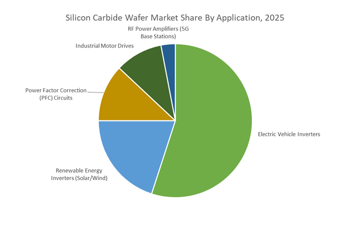
SiC is also the essential semiconductor technology enabling the automotive industry’s rapid move toward 800-volt architectures, which dramatically reduce charging time and improve powertrain efficiency. Higher voltage operation reduces current for a given power level, enabling lighter wiring harnesses, smaller magnetic components, and more compact inverter designs. In fast-charging scenarios, SiC-based inverters and onboard chargers allow EVs to reach 80% battery capacity within 15–20 minutes, a critical milestone for mass-market adoption. As global automakers and Tier-1 suppliers standardize SiC devices across premium and mid-range EV platforms, the wafer demand for SiC continues to surge. Combined with rising EV sales, aggressive OEM electrification roadmaps, and government mandates accelerating the transition away from internal combustion engines, EV inverters remain the dominant and fastest-growing application for SiC wafers worldwide.
Country Analysis: Global SiC Wafer and Substrate Manufacturing Hubs
United States – CHIPS Act–Enabled Expansion of the World’s First High-Volume 200mm Silicon Carbide Wafer Manufacturing Ecosystem
The United States remains at the forefront of the global Silicon Carbide Wafer Market, setting the pace in SiC substrate innovation, 200mm wafer scaling, and vertically integrated wide bandgap semiconductor production. The catalytic force behind this leadership is the unprecedented federal support under the CHIPS and Science Act, which is directly accelerating the shift toward next-generation 200mm SiC wafer manufacturing. In October 2024, the U.S. Department of Commerce signed a PMT with Wolfspeed to provide up to $750 million in CHIPS Act funding, marking one of the largest government-backed investments in SiC materials globally.
The investment underpins the construction of the John Palmour Manufacturing Center in Siler City, North Carolina, which is positioned to become the United States’ largest SiC wafer manufacturing hub and the world’s first high-volume 200mm SiC wafer fab. Designed to deliver more than a tenfold increase in SiC wafer output over Wolfspeed’s Durham campus, the facility will exclusively produce 200mm substrates to feed the company’s fast-growing device fabs. Wolfspeed activated its initial furnaces at Siler City in 2024 and is on track to begin supplying 200mm SiC wafers to the Mohawk Valley 200mm device fab by mid-2025, achieving a seamless pipeline from substrate to finished power devices. These developments firmly establish the U.S. as the global leader in next-generation 200mm SiC wafer scaling, substrate quality innovations, and large-scale electrification materials.
China – Rapid Domestic Substitution and 8-Inch SiC Wafer Expansion Driven by Automotive and EV Electrification
China is executing one of the world’s most aggressive scale-up programs in 8-inch (200mm) SiC wafer manufacturing, driven by strategic government funding, vertically integrated industrial ecosystems, and fast-growing domestic EV demand. A centerpiece of this expansion is Sanan Optoelectronics’ Chongqing 8-inch SiC substrate line, supported by an investment of approximately CNY 7 billion (nearly $1 billion). The line began production in September 2024 and is designed to rapidly increase domestic supply of high-quality 200mm SiC substrates, addressing China’s long-term dependency on foreign wafer suppliers.
China’s leadership in vertically integrated SiC manufacturing strengthened further with the STMicroelectronics–Sanan joint venture, inaugurated in February 2025. The JV will operate an 8-inch SiC device fab in Chongqing targeting volume production by Q4 2025, specifically aligned with China’s surging EV power electronics market. The fab’s fully ramped production capacity—10,000 automotive-grade 200mm wafers per week—marks one of the largest automotive SiC production commitments globally. The regional pairing of Sanan’s substrate line + ST/Sanan’s device fab creates a fully self-sustaining SiC manufacturing ecosystem, enabling China to accelerate domestic substitution and cement its role as a global powerhouse in high-volume SiC wafer manufacturing for EV traction inverters, industrial drives, and renewable applications.
Japan – Materials Science Leadership and Strategic Shift Toward 8-Inch SiC Wafer Commercialization
Japan continues to prioritize its long-established expertise in high-purity SiC substrates and advanced semiconductor materials, while strategically transitioning toward large-diameter 8-inch wafer production. In December 2025, Mitsubishi Electric completed construction of its new 8-inch SiC wafer front-end fab in Kikuchi, Kumamoto Prefecture, marking a major milestone in Japan’s wide bandgap semiconductor roadmap. The facility is set for full-scale mass production in 2027 and will significantly expand Mitsubishi’s SiC portfolio for EV powertrains, industrial automation, and advanced energy equipment.
To strengthen supply-chain resilience, Mitsubishi Electric allocated part of its long-term ¥260 billion investment plan to SiC material security, including a $500 million investment into a newly carved-out Coherent Corp. SiC business, guaranteeing stable access to 200mm n-type 4H SiC substrates. Complementing industry commitments, the Japanese government—through the Ministry of Economy, Trade, and Industry (METI)—provides tax credits and targeted subsidies to accelerate domestic production of SiC materials and wafers. This cohesive ecosystem positions Japan as a critical supplier of high-reliability 8-inch SiC wafers and advanced semiconductor materials essential for next-generation electrification.
South Korea – Converting Legacy Semiconductor Lines into High-Volume 200mm SiC Wafer Manufacturing Platforms
South Korea is rapidly expanding its role in the Silicon Carbide Wafer Market, leveraging its established high-volume semiconductor infrastructure to scale 200mm SiC wafer production. In October 2023, Onsemi completed the expansion of its Bucheon SiC facility, equipped to manufacture more than one million 200mm SiC wafers annually—a capacity that ranks among the largest globally. The facility currently processes 150mm wafers but is scheduled for a full conversion to 200mm SiC wafer production in 2025, marking a major step in Korea’s transition to large-diameter wide bandgap semiconductor manufacturing.
South Korea is also developing a strong foundry-based SiC ecosystem. SK keyfoundry is actively creating 1200V SiC MOSFET processes, with a dedicated SiC foundry service expected to launch in the first half of 2026. This development is set to open new domestic and international channels for SiC wafer demand. Complementing industrial expansion, the South Korean government has established a strategic goal to achieve 20% self-sufficiency in SiC power semiconductors by 2030, directly accelerating investment in materials, wafer processing, and device fabrication. These initiatives position South Korea as an emerging leader in high-volume, automotive-grade 200mm SiC wafer production and SiC MOSFET foundry services.
Competitive Landscape: Global Leaders in SiC Substrates, Epitaxy, and Crystal Growth Technologies
The Silicon Carbide wafer market is dominated by companies that maintain deep expertise in crystal growth, epitaxy, substrate polishing, and wafer-scale quality consistency. Vertical integration and R&D-intensive scaling strategies remain the primary competitive differentiators as the industry transitions toward 200 mm and future 300 mm wafers.
Wolfspeed remains the most influential SiC wafer manufacturer globally, holding leadership in boule growth, substrate fabrication, and MOSFET device production. In 2025, the company successfully transitioned to commercial 200 mm wafer qualification, directly supporting large-scale EV and industrial power system production requirements. Its Gen 4 MOSFET platform, launched in January 2025, demonstrates how Wolfspeed converts wafer-level improvements into high-efficiency power devices. The company’s strategic emphasis remains centered on long-term supply agreements with automotive OEMs and Tier-1 traction inverter suppliers.
Coherent Corp. (formerly II-VI) is a premier supplier of high-performance SiC substrates specializing in advanced crystal growth and wafer polishing. In December 2025, it announced a breakthrough expansion into 300 mm SiC substrate development, positioning the company as a technology leader in next-generation wafer scaling. Coherent primarily serves IDMs that lack internal substrate capability, enabling high-quality material provision across power electronics and GaN-on-SiC RF applications used in 5G and aerospace.
Sumitomo Electric leverages its proprietary MPZ™ (Multi-Point Seeded Growth) technology to achieve world-class uniformity and reduced defect density in SiC crystals. The company’s epitaxial wafers consistently demonstrate more than 99% defect-free area, a key performance metric for high-voltage automotive and industrial devices. Sumitomo is also advancing VMOSFETs capable of 200 A per chip, reflecting its dual strategy of wafer innovation and device-level integration. Its focus centers on enabling high-efficiency power systems and supporting global sustainability targets.
SK Siltron significantly enhanced its SiC position through its acquisition of DuPont’s SiC wafer unit, operating under SK Siltron CSS. Leveraging SK Group’s broad semiconductor materials expertise, the company applies silicon wafer process excellence—crystal purity, flatness, and surface control—to strengthen its SiC substrate quality. SK Siltron’s production roadmap aligns with its Net Zero 2040 target, focusing on energy-efficient wafer manufacturing and supporting the rapidly expanding EV and industrial WBG markets.
TanKeBlue is one of China’s earliest national high-tech SiC substrate enterprises and is rapidly expanding its global footprint. In August 2025, it began construction on its Phase II expansion to increase wafer output to 230,000 pieces by August 2026, strengthening China’s domestic SiC supply chain. The company previously secured a multi-year supply agreement with Infineon (May 2023) for both 150 mm and 200 mm wafers, validating its material quality. TanKeBlue’s applications extend across NEVs, wind energy, solar inverters, ESS systems, and 5G, positioning it as a strategically important player in Asia.
Silicon Carbide Wafer Market
|
Parameter
|
Details
|
|
Market Size (2025)
|
$1.1 Billion
|
|
Market Size (2035)
|
$7.8 Billion
|
|
Market Growth Rate
|
21.7%
|
|
Segments
|
By Wafer Size (4-inch, 6-inch, 8-inch), By Material Type (Conductive SiC Substrates, Semi-Insulating SiC Substrates), By Product Form (Bare Substrates, Polished Wafers, Epitaxial Wafers), By Polytype (4H-SiC, 6H-SiC, 3C-SiC), By Application of Final Device (EV Inverters, Renewable Energy Inverters, Industrial Motor Drives, Power Factor Correction Circuits, RF Power Amplifiers)
|
|
Study Period
|
2019- 2024 and 2025-2034
|
|
Units
|
Revenue (USD)
|
|
Qualitative Analysis
|
Porter’s Five Forces, SWOT Profile, Market Share, Scenario Forecasts, Market Ecosystem, Company Ranking, Market Dynamics, Industry Benchmarking
|
|
Companies
|
Wolfspeed Inc., Coherent Corp., ROHM Co. Ltd., Resonac Corporation, SK Siltron Co. Ltd., Sanan Optoelectronics Co. Ltd., Tankeblue Semiconductor Co. Ltd., II-VI Incorporated, Kyocera Corporation, WeEn Semiconductors Co. Ltd., Infineon Technologies AG, STMicroelectronics N.V.
|
|
Countries
|
US, Canada, Mexico, Germany, France, Spain, Italy, UK, Russia, China, India, Japan, South Korea, Australia, South East Asia, Brazil, Argentina, Middle East, Africa
|
Silicon Carbide Wafer Market Segmentation
By Wafer Size
- 4-inch (100mm)
- 6-inch (150mm)
- 8-inch (200mm)
By Material Type
- Conductive SiC Substrates (N-type)
- Semi-Insulating SiC Substrates
By Product Form
- Bare Substrates (SiC Boules)
- Polished Wafers
- SiC Epitaxial Wafers
By Polytype
By Application of Final Device
- Electric Vehicle Inverters
- Renewable Energy Inverters (Solar/Wind)
- Industrial Motor Drives
- Power Factor Correction (PFC) Circuits
- RF Power Amplifiers (5G Base Stations)
By Region
- North America (United States, Canada, Mexico)
- Europe (Germany, France, United Kingdom, Spain, Italy, Rest of Europe)
- Asia Pacific (China, India, Japan, South Korea, Australia, Rest of APAC)
- South and Central America (Brazil, Argentina, Rest of SCA)
- Middle East and Africa (Saudi Arabia, UAE, South Africa, Rest of Middle East, Rest of Africa)
Top Companies: Key Silicon Carbide Wafer and Material Suppliers
- Wolfspeed, Inc.
- Coherent Corp.
- ROHM Co., Ltd.
- Resonac Corporation (Showa Denko)
- SK Siltron Co., Ltd.
- Sanan Optoelectronics Co., Ltd.
- Tankeblue Semiconductor Co., Ltd.
- II-VI Incorporated
- Kyocera Corporation
- WeEn Semiconductors Co., Ltd.
- Infineon Technologies AG
- STMicroelectronics N.V. (ST)
*- List not Exhaustive
