Compound Semiconductor Materials Market Overview: Wide Bandgap Breakthroughs Powering EVs, 5G Infrastructure & High-Efficiency Power Electronics
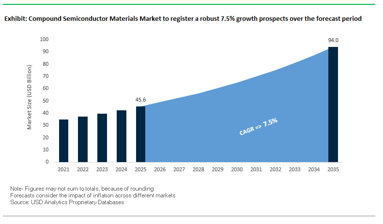
The Compound Semiconductor Materials Market, valued at USD 45.6 billion in 2025 and projected to reach USD 94 billion by 2035 at a strong 7.5% CAGR, is accelerating into a hyper-growth phase as Wide Bandgap (WBG) materials—Silicon Carbide (SiC) and Gallium Nitride (GaN)—become foundational to the future of energy-efficient systems, high-frequency communications, and next-generation mobility. These materials deliver 10× higher breakdown voltage, 3–5× higher electron mobility, superior thermal conductivity, and dramatically faster switching speeds compared with silicon, pushing OEMs and power-electronics designers to redesign entire platforms around WBG capabilities.
As global industries shift toward 800V EV architectures, ultra-fast charging, 5G/6G network densification, high-power radar, renewable energy inverters, AI data-center power supplies, and high-temperature industrial controls, compound semiconductors are rapidly becoming indispensable. Their system-level benefits—>50% power-loss reduction in EV inverters, higher RF efficiency for 5G massive-MIMO, reduced cooling requirements, and smaller, lighter power systems—are reshaping procurement priorities and long-term technology roadmaps across automotive, telecom, defense, and semiconductor ecosystems. The next decade marks the transition from silicon-limited performance to WBG-enabled electrification and high-frequency infrastructure, positioning compound semiconductors as one of the most strategically important material classes through 2035.
Market Analysis: Strategic SiC Capacity Expansions, GaN Defense Validation & High-Volume 200 mm Scaling
The compound semiconductor materials market experienced a decisive shift in 2025 as leading suppliers scaled production, OEMs accelerated EV electrification roadmaps, and 5G/defense programs validated GaN’s high-frequency superiority. In December 2025, Wolfspeed secured a substantial USD 698.6 million tax refund, which directly strengthens capital allocation for its 200 mm SiC wafer and device manufacturing expansion. The strategic importance of 200 mm substrates cannot be overstated - larger wafer diameters materially reduce cost per die, improve output per batch, and help alleviate persistent supply constraints in the EV and industrial markets.
The surge in SiC device launches continued through September 2025, when Infineon expanded its CoolSiC MOSFET portfolio with new 400 V and 440 V variants, opening new pathways for industrial drives and mid-voltage automotive platforms. In the same month, Aixtron shipped its 100th G10-SiC epitaxy system, a milestone illustrating the explosive need for epi-growth capacity. Also in September 2025, Epirus demonstrated the real-world performance of GaN-based defense systems by neutralizing all 61 airborne drone targets using its Leonidas high-power microwave system - a validation that positions GaN as the premier material for high-power, fast-switching defense and aerospace systems.
Government and regional semiconductor industrial policies are increasingly shaping market expansion. In August 2025, India approved four compound semiconductor projects under the India Semiconductor Mission, including a landmark collaboration with Clas-SiC Wafer Fab (UK) to build India’s first commercial SiC fab with 60,000-wafer annual capacity. This follows accelerating EV infrastructure-related commitments, bolstered by Infineon’s collaboration with e-Drift Electric (August 2025) to deploy Si–SiC-MOSFET integrated solutions for fast-charging.
Industry consolidation and vertical integration further intensified in February 2025, with Infineon completing its acquisition of GaN Systems, ensuring dominant influence in the Power GaN value chain. Meanwhile, Wolfspeed’s September 2025 introduction of 200 mm SiC materials marks a historic inflection point for cost competitiveness, supply stability, and device-scaling efficiency across the automotive, industrial and renewable energy markets.
Trends and Opportunities Transforming Scale, Architecture, and Material Selection in the Compound Semiconductor Materials Market
Trend 1: Multi-Billion-Dollar Vertical Integration for 200 mm SiC Epitaxy as EV OEMs Demand Supply Certainty and Cost Reduction
The transition from 150 mm to 200 mm SiC wafer technology is the centerpiece of global investment strategies among automotive, semiconductor, and power module manufacturers. This scale jump is not merely a technical upgrade—it is the economic enabler for meeting explosive demand for SiC MOSFETs and diodes in high-voltage EV architectures.
Increasing wafer diameter from 150 mm to 200 mm expands usable die area by 1.8–1.9×, dramatically lowering cost-per-ampere and improving throughput for high-volume EV platforms. This shift is visible in Wolfspeed’s $1 billion Mohawk Valley 200 mm fab investment and STMicroelectronics’ multi-year expansion roadmap. These investments are tightly linked to the strategic intent of OEMs such as Volkswagen, which has signed multi-billion-dollar SiC power module supply agreements with onsemi. In parallel, onsemi’s vertically integrated SiC manufacturing facility in the Czech Republic is on track to qualify 200 mm SiC wafers, positioning the company to meet the EV industry’s long-term powertrain requirements.
The ecosystem-scale investments signal the market’s pivot toward complete end-to-end SiC control—from bulk crystal growth to epitaxy, device fabrication, and module assembly—ensuring supply security and enabling the price reductions needed to mainstream SiC in mass-market EVs.
Trend 2: Commercialization of GaN-on-Silicon as a Cost-Optimized Platform for Fast Charging and Sub-6 GHz 5G RF
Gallium Nitride is rapidly moving from niche high-frequency applications into mainstream consumer electronics and telecom infrastructure, thanks to the cost advantages of GaN-on-Silicon (GaN-on-Si). By leveraging mature, depreciated 200 mm silicon fabs, GaN-on-Si technology enables dramatic improvements in performance, size, and efficiency without incurring the premium manufacturing costs associated with sapphire or SiC substrates.
In consumer power delivery, GaN-on-Si chargers deliver up to 3× faster charging in form factors that are 50% smaller and lighter, accelerating adoption across smartphones, laptops, and high-performance accessories. The move to 200 mm substrates yields 2.3× more die per wafer compared to 150 mm, further reducing cost-per-watt and enabling high-volume commercialization.
In telecom infrastructure, GaN-on-Si devices deliver 3–6× higher power density than GaAs or Si-LDMOS, an essential advantage for the tens of thousands of 5G base stations deploying each quarter. These attributes position GaN-on-Si as a foundational material for sub-6 GHz 5G radios, consumer fast chargers, and emerging wireless power applications.
Opportunity 1: Native GaN Substrates Unlock High-Efficiency UV-C LEDs and Micro-LED Displays with Drastically Lower Defect Density
The limitations of heteroepitaxial GaN growth (such as GaN-on-sapphire or GaN-on-Si), particularly high threading dislocation density (TDD ~10⁹ cm⁻²), constrain performance in UV-C LEDs and Micro-LEDs. This creates a high-value opportunity for native GaN substrates (GaN-on-GaN) that dramatically reduce TDD to the 10⁶ cm⁻² range, enabling transformative improvements in efficiency and stability.
For UV-C disinfection LEDs, reducing non-radiative recombination centers is essential to achieving long lifetimes and high external quantum efficiency. Native GaN substrates directly address this, overcoming degradation issues that currently limit UV-C LED lifetimes to only a few thousand hours.
In Micro-LEDs—critical for AR displays—devices grown on native GaN maintain superior luminous efficiency at high current densities (up to 200 A/cm²), effectively mitigating the “efficiency droop” phenomenon. Native GaN also offers low resistivity, enabling vertical LED and VCSEL architectures that provide superior heat dissipation and uniform current spreading compared to traditional lateral devices.
The shift positions native GaN substrates as one of the highest-value material opportunities across optoelectronics over the next decade.
Opportunity 2: Ultra-Wide Bandgap Materials (Ga₂O₃ and AlN) Create New Frontiers for Extreme-Voltage, Extreme-Temperature Power Electronics
Beyond SiC and GaN, the next wave of power electronics innovation is emerging from Ultra-Wide Bandgap (UWBG) materials, particularly β-Gallium Oxide (Ga₂O₃) and Aluminum Nitride (AlN), which promise unprecedented voltage, temperature, and efficiency capabilities.
β-Ga₂O₃ offers a theoretical breakdown field of ~8 MV/cm, enabling power devices with voltage ratings far exceeding SiC or GaN. Early prototypes demonstrate 8.5 kV breakdown voltages, validating its potential for HVDC grid systems and industrial power conversion. Critically, Ga₂O₃ is the only UWBG material that can be melt-grown via low-cost Czochralski methods, giving it a long-term cost advantage over SiC and GaN substrates.
Aluminum Nitride (AlN), with its combination of high thermal conductivity and extreme chemical stability, is emerging as a substrate for electronics operating at temperatures >1000°C, making it suitable for jet engine sensors, UAV propulsion monitoring, and downhole drilling electronics. AlN enables robust device performance in operating environments that exceed the functional limits of SiC and GaN.
These UWBG materials represent the next disruptive opportunity for ultra-high-power, high-temperature, and high-frequency electronics serving aerospace, defense, renewable energy, and advanced grid infrastructure.
Compound Semiconductor Materials Market Share Analysis
Market Share by Material Type: Silicon Carbide (SiC) Leads with 46.1% Share
Silicon Carbide (SiC) dominates the Compound Semiconductor Materials Market with a 46.1% share in 2025, firmly establishing itself as the backbone of the global wide-bandgap semiconductor transition. Its leadership is driven by SiC’s unmatched performance in high-voltage, high-temperature, and high-efficiency power applications, making it indispensable for electric vehicle (EV) traction inverters, onboard chargers, renewable energy inverters, and industrial power modules. SiC’s first-mover advantage—particularly its early qualification by automotive OEMs—has created a steep barrier to entry for competing materials, enabling SiC to scale rapidly as EV penetration accelerates worldwide. The broader material landscape reinforces SiC’s strategic positioning: Gallium Nitride (GaN) is rising as the dominant material for high-frequency and medium-voltage power conversion, GaAs and InP continue to anchor niche but high-value photonics and RF segments, and emerging materials like Ga₂O₃ and CdTe signal the next frontier for ultra-high breakdown voltage and thin-film photovoltaic systems. Collectively, the segmentation illustrates a market where SiC leads the electrification wave, GaN reshapes RF and low-power conversion, and legacy III–V materials sustain stronghold positions in specialized applications.
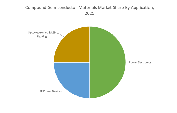
Market Share by Application: Power Electronics Lead with 51.1% Share
Power Electronics account for the largest share at 51.1% in 2025, reflecting their pivotal role in global electrification and energy-efficiency transformation. This segment dominates because compound semiconductors—particularly SiC and GaN—deliver substantial improvements in power density, switching efficiency, thermal conductivity, and voltage handling, enabling the next generation of EV drivetrains, renewable energy systems, energy storage, and high-reliability industrial drives. The segment’s outsized share is driven by the explosive adoption of SiC MOSFETs in EV traction inverters, the acceleration of GaN-based fast chargers and onboard chargers, and the increasing electrification of industrial machinery and grid infrastructure. Meanwhile, RF power devices represent a fast-scaling, high-margin market reshaped by GaN’s superior high-frequency and high-power performance, driving widespread transition from GaAs and silicon LDMOS as 5G/6G networks proliferate. Optoelectronics, while more mature, remains foundational to fiber-optic communications, sensing, LiDAR, LED lighting, and display innovations.
Country Analysis: Global Compound Semiconductor Materials Market Innovation Hubs
United States: CHIPS Act–Driven SiC/GaN Capacity Expansion and Vertical Integration for Power Electronics Leadership
The United States has emerged as one of the most aggressive investors in compound semiconductor materials, channeling billions through the CHIPS and Science Act to secure domestic manufacturing of Silicon Carbide (SiC) and Gallium Nitride (GaN) substrates. These investments target national supply chain resilience and the strategic scaling of wide-bandgap (WBG) power electronics vital for electric vehicles, industrial automation, defense platforms, and 5G/6G communication systems. The government’s prioritization of compound semiconductors extends beyond subsidies—its policies directly support ecosystem development, workforce expansion, and high-volume substrate production.
A core beneficiary of this national strategy is Wolfspeed, the world’s only pure-play, vertically integrated SiC company. Wolfspeed received $698.6 million in Section 48D Cash Tax Refunds (Dec 2025), accelerating its expansion into 200mm SiC wafer manufacturing, enabling cost reductions and dramatically scaling SiC supply for the global e-mobility propulsion market. In parallel, the company’s launch of 1200V SiC Six-Pack Power Modules (Nov 2025) showcases the performance breakthroughs achievable with advanced SiC materials for EV inverters and drivetrains. Further strengthening the technological ecosystem, the National Science Foundation (NSF) committed $25 million to secure communication technologies for 5G and 6G, reinforcing U.S. leadership in GaN RF devices. Meanwhile, the Aerospace and Defense sector remains a cornerstone market, leveraging GaN for high-power radar and electronic warfare, where device reliability under extreme heat and frequency loads is critical.
China: National Localization Strategy and EV-Driven SiC Demand Under Big Fund III
China’s compound semiconductor materials market is shaped by highly coordinated state policy, placing semiconductor self-sufficiency at the center of national industrial strategy. The 14th Five-Year Plan identifies Integrated Circuits—including SiC and GaN power semiconductors—as strategic technology areas, with mandates to localize critical materials, process tools, and equipment. This aligns with China’s broader move to reshape its domestic semiconductor base through capital-intensive buildouts supported by national and provincial governments.
A pivotal development is the launch of Big Fund Phase III (2024), injecting significant financing into domestic capacity for SiC wafer production, epitaxy, and device fabrication, enabling China to close gaps with leading global suppliers. This is strongly reinforced by China’s dominant electric vehicle ecosystem, which is the world’s largest consumer of SiC MOSFETs used in high-efficiency traction inverters and onboard chargers. As automakers deploy SiC into mass-market models, local suppliers are racing to vertically integrate from substrates to modules. Concurrently, China’s telecom leadership ensures sustained demand for GaN power amplifiers as the country accelerates the rollout of 5G base stations—one of the largest application segments for compound semiconductor RF devices. The resulting wave of M&A consolidation (10+ deals in 2025) signals a transformation toward end-to-end domestic manufacturing, reducing reliance on foreign materials and equipment.
European Union: Chips Act–Backed WBG Innovation and GaN Industrialization Across Strategic Member States
The European Union is mobilizing a coordinated, long-term vision to double its share of global semiconductor production through the European Chips Act, emphasizing wide-bandgap materials (SiC, GaN) and advanced compound semiconductor technologies. With €43 billion in combined public–private investment, the EU aims to establish advanced pilot lines, accelerate industrialization, and ensure strategic autonomy in power semiconductors and RF technologies. Member states, research institutes, and industrial consortia are working collaboratively under this framework.
A major development is the formation of the EU Semiconductor Coalition (March 2025), led by nine key member states including Germany, France, and Italy. This coalition coordinates infrastructure investment, R&D funding, and cross-border production strategies to enhance Europe’s competitive position in compound semiconductor materials. Leading EU manufacturer Infineon Technologies AG announced plans to roll out 12-inch GaN substrate samples by Q4 2025, a game-changing shift that will reduce device cost and accelerate GaN’s penetration into EV traction inverters, industrial drives, and renewable energy systems. Meanwhile, Poland’s Semiconductor Industry Development Strategy (Feb 2025) introduces incentives to attract wafer fabrication and material science companies, aligning the country with EU-wide industrial-scale semiconductor expansion. Collectively, these initiatives position the EU as a rising force in SiC and GaN R&D, manufacturing, and power electronics integration.
Japan: Precision Materials Leadership in SiC and GaN for Global Automotive and RF Applications
Japan remains a global powerhouse in compound semiconductor materials, particularly in high-quality SiC substrates, GaN epitaxy, and advanced lithography materials. The country’s materials science ecosystem—built on decades of expertise in crystal growth, wafer polishing, and high-reliability electronics—enables Japan to supply some of the most demanding end markets, including automotive power modules, industrial automation, and 5G/6G communication systems.
Japanese leaders like ROHM Co., Ltd. and Sumitomo Electric Industries are transitioning their SiC and GaN platforms to 200mm wafer formats, a critical step in reducing cost per ampere and achieving mass-market scalability for EV power electronics. This positions Japan to maintain its advantage in ultra-high reliability SiC for automotive OEMs worldwide. Complementing this shift, Shin-Etsu Chemical Co. committed approximately $560 million through 2026 to expand lithography materials production, reinforcing its essential role in the advanced semiconductor supply chain. In RF technology, Sumitomo Electric’s GaN HEMT devices remain globally recognized for their high-frequency efficiency and reliability, supporting next-generation telecommunications infrastructure. Together, Japan’s leadership in materials innovation and precision manufacturing solidifies its strategic importance in the global compound semiconductor landscape.
Competitive Landscape: Vertically Integrated SiC Leaders & RF GaN Powerhouses Driving Next-Gen Electronics
The competitive landscape for Compound Semiconductor Materials is shaped by deep vertical integration (from substrate to module), leadership in epitaxy and wafer scaling, and dominance in RF GaN and SiC power semiconductors. Success hinges on securing high-purity substrates, controlling defect-density, and enabling high-volume manufacturing compatible with 200 mm platforms.
Wolfspeed, Inc. - The Global Leader in Vertically Integrated Silicon Carbide
Wolfspeed remains the world’s only pure-play SiC company, controlling the full supply chain from bare SiC wafer → epitaxy → MOSFETs/modules. The company’s strategic acceleration of 200 mm capacity - funded partly through a USD 698.6M tax refund (Dec 2025) - positions it as the most scalable supplier of SiC materials globally. Wolfspeed’s SiC MOSFETs operate continuously at 185°C junction temperature and support 650–1700 V voltage ratings, optimized for EV traction inverters, renewables and industrial drives. This vertical integration ensures predictable material quality, device consistency and long-term supply reliability.
Infineon Technologies AG - Power Electronics Leader Scaling SiC & GaN at Global Volumes
Infineon is a dominant force in SiC (CoolSiC™) and GaN (CoolGaN™) device technologies, backed by multi-billion-dollar investments including its €5B Kulim 200 mm SiC Mega Fab. Its Feb 2025 acquisition of GaN Systems strengthens its leadership in RF and power GaN. The company uses its proprietary Cold Split SiC materials process to optimize wafer utilization, while its GaN devices are already deployed in high-efficiency power adapters (e.g., 250W PoE adapter announced Sep 2025). Infineon also collaborates with ROHM (Sep 2025) to advance next-generation SiC packaging.
Qorvo, Inc. - Global Leader in GaAs/GaN RF Solutions for 5G & Defense
Qorvo maintains leadership in GaN and GaAs materials for RF front-end modules, phased array radar, satellite communication, and 5G infrastructure. GaN’s superior electron mobility and high-power density enable Qorvo’s RF power amplifiers to deliver unmatched linearity and signal integrity for massive MIMO and defense radar systems. Qorvo’s foundry capabilities and GaN-based FEMs position it as a critical supplier for high-frequency, high-reliability markets where silicon is no longer competitive.
ROHM Co., Ltd. - High-Reliability SiC MOSFET and SBD Manufacturer Driving Packaging Innovation
ROHM is a leading innovator in SiC MOSFETs, SiC SBDs, and compact molded SiC modules. Its DOT-247 2-in-1 SiC molded module (Sep 2025) underlines its focus on improving manufacturability and thermal performance. The company also entered a strategic packaging collaboration with Infineon (Sep 2025) to standardize next-generation SiC module formats. ROHM’s devices support high-temperature, high-frequency switching required in EV onboard chargers, solar inverters and industrial motor drives.
NIPPON SHOKUBAI CO. LTD - Critical Supplier of High-Purity Organometallic Precursors for GaN & AlN Epitaxy
Nippon Shokubai plays an essential role upstream by supplying Trimethylaluminum (TMA) and other ultra-high-purity precursors required for MOCVD growth of GaN and AlN. The company is expanding its precursor manufacturing footprint to support explosive global demand for GaN HEMT devices used in 5G RF systems and radar. Its precursors enable low-defect, uniform epitaxial layers - a key differentiator for device yield and RF performance.
Compound Semiconductor Materials Market
|
Parameter
|
Details
|
|
Market Size (2025)
|
$45.6 Billion
|
|
Market Size (2035)
|
$94 Billion
|
|
Market Growth Rate
|
7.5%
|
|
Segments
|
By Material Type (III–V Semiconductors, IV–IV Semiconductors, II–VI Semiconductors, Emerging Materials), By Device Structure (HEMTs, MOSFETs, IGBTs, Schottky Diodes, Laser Diodes, LEDs), By Application (Power Electronics, RF Power Devices, Optoelectronics, LED Lighting), By Wafer Size (100 mm, 150 mm, 200 mm)
|
|
Study Period
|
2019- 2024 and 2025-2034
|
|
Units
|
Revenue (USD)
|
|
Qualitative Analysis
|
Porter’s Five Forces, SWOT Profile, Market Share, Scenario Forecasts, Market Ecosystem, Company Ranking, Market Dynamics, Industry Benchmarking
|
|
Companies
|
Wolfspeed Inc., STMicroelectronics N.V., Infineon Technologies AG, ROHM Co. Ltd., Sumitomo Electric Industries Ltd., Qorvo Inc., onsemi, MACOM Technology Solutions Holdings Inc., Mitsubishi Electric Corporation, Toshiba Electronic Devices & Storage Corporation, Navitas Semiconductor Corporation, IQE plc, GlobalFoundries, II-VI Incorporated, WIN Semiconductors Corp.
|
|
Countries
|
US, Canada, Mexico, Germany, France, Spain, Italy, UK, Russia, China, India, Japan, South Korea, Australia, South East Asia, Brazil, Argentina, Middle East, Africa
|
Compound Semiconductor Materials Market Segmentation
By Material Type
- III–V Semiconductors
- IV–IV Semiconductors
- Emerging Materials
- II–VI Semiconductors
By Device Structure
- High Electron Mobility Transistors (HEMTs)
- Metal-Oxide-Semiconductor Field-Effect Transistors (MOSFETs)
- Insulated Gate Bipolar Transistors (IGBTs)
- Schottky Diodes
- Laser Diodes (LD)
- Light-Emitting Diodes (LEDs)
By Application
- Power Electronics
- RF Power Devices
- Optoelectronics
- LED Lighting
By Wafer Size
- 150 mm (6-inch) Substrates
- 200 mm (8-inch) Substrates
- 100 mm (4-inch) Substrates
By Region
- North America (United States, Canada, Mexico)
- Europe (Germany, France, United Kingdom, Spain, Italy, Rest of Europe)
- Asia Pacific (China, India, Japan, South Korea, Australia, Rest of APAC)
- South and Central America (Brazil, Argentina, Rest of SCA)
- Middle East and Africa (Saudi Arabia, UAE, South Africa, Rest of Middle East, Rest of Africa)
Top Companies in the Compound Semiconductor Materials Market
- Wolfspeed, Inc.
- STMicroelectronics N.V.
- Infineon Technologies AG
- ROHM Co., Ltd.
- Sumitomo Electric Industries, Ltd.
- Qorvo, Inc.
- onsemi
- MACOM Technology Solutions Holdings, Inc.
- Mitsubishi Electric Corporation
- Toshiba Electronic Devices & Storage Corporation
- Navitas Semiconductor Corporation
- IQE plc
- GlobalFoundries
- II-VI Incorporated
- WIN Semiconductors Corp.
*- List not Exhaustive
