
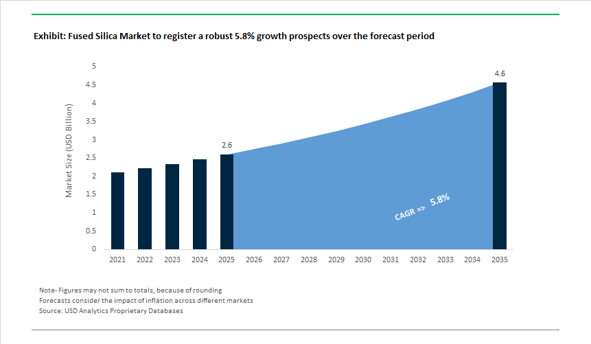
The Fused Silica Market, valued at USD 2.6 billion in 2025 and projected to reach USD 4.6 billion by 2035 at a 5.8% CAGR, is increasingly defined by its system-critical role in semiconductor manufacturing, advanced optics, and high-frequency electronics rather than by volume growth alone. Its strategic relevance today is driven by the fact that yield loss, overlay error, and thermal drift at advanced technology nodes are no longer dominated by equipment mechanics but by substrate-level material stability. In EUV lithography, photomask substrates, wafer carriers, lens elements, and process chamber components rely on fused silica to deliver near-zero thermal expansion, deep-UV transparency, and chemical inertness under continuous thermal cycling and plasma exposure. For OEMs, fused silica performance directly translates into tool uptime, overlay accuracy, and long-term capital efficiency.
Market demand is being reshaped by a structural shift toward tighter impurity control and dimensional predictability as chipmakers scale below 5 nm and push higher numerical aperture (High-NA) EUV systems. Leading manufacturers are engineering synthetic fused silica with ppb-level metallic impurity thresholds, ultra-low hydroxyl (OH) content for laser and photomask applications, and CTE stability measured in parts per billion per °C, ensuring minimal thermal distortion during high-energy exposure. In parallel, 300 mm wafer processing has standardized extreme flatness and homogeneity requirements, while roadmap discussions around 450 mm wafer tools further elevate the importance of refractive index uniformity and bulk homogeneity across large formats. Outside semiconductors, high-power laser optics and 5G/mmWave dielectric components are reinforcing demand for low dielectric loss and high damage-threshold silica grades, expanding the market beyond pure lithography dependency.
Further, fused silica continues to displace alternative glass and ceramic materials where process stability outweighs raw material cost. Its ability to maintain optical clarity, dimensional accuracy, and dielectric performance over long service intervals reduces recalibration frequency, extends component life, and lowers total cost of ownership for fabs and laser system integrators. Looking ahead, market leadership will consolidate around suppliers capable of vertically controlled synthesis, tight batch-to-batch reproducibility, and application-specific grading aligned with semiconductor equipment qualification cycles. As fabs prioritize material traceability, contamination control, and long-term supply security, fused silica is set to remain a non-substitutable enabler of advanced manufacturing, anchoring steady, high-value growth through 2035.
Market dynamics in 2025 highlight the strengthening role of fused silica in semiconductor lithography, optical fiber manufacturing, and next-generation energy technologies. In Dec 2025, Tosoh Corporation announced a substantial strategic shift toward silica glass production to meet surging demand from AI hardware, EV power electronics, and 5G RF systems, signaling long-term structural growth in high-purity silica consumption. Earlier, in Nov 2025, Heraeus Covantics introduced its improved HSQ® electrically fused quartz line designed for next-generation 12-inch wafer tools, offering enhanced thermal stability and chemical purity to support aggressive node scaling. Reinforcing this semiconductor orientation, Oct 2025 saw Corning certify that its HPFS® grades now achieve Inclusion Class 0 and extremely low birefringence-performance metrics indispensable for advanced ArF/193 nm lithography.
In Sep 2025, Shin-Etsu Quartz completed capacity expansion for large-size synthetic quartz photomask substrates and display glass, supporting growing demand from flat-panel and semiconductor applications where high homogeneity and defect-free structures are critical. The energy transition also influenced market dynamics: Aug 2025 saw Momentive Technologies secure a long-term contract to supply ultra-pure quartz crucibles for silicon crystal pulling in solar cell manufacturing, reflecting strong renewable energy adoption.
Laser systems and fiber optics also remained key growth pillars. Jun 2025 delivered an R&D breakthrough with published findings showing a 25% improvement in fused silica laser damage thresholds at 1064 nm, accelerating its adoption in high-power fiber lasers for industrial cutting and precision machining. In Apr 2025, Heraeus expanded its HP quartz tube line with improved ovality tolerances (0.01-0.03 mm), enhancing performance in optical fiber preforms. On the other hand, Feb 2025 marked Nikon’s announcement of its NIFS synthetic silica performance for lithography lenses, engineered for low OH content and exceptional homogeneity-reinforcing fused silica’s role in leading-edge semiconductor optics.
The migration to High-NA EUV lithography (0.55 NA) has elevated fused silica from a passive optical substrate to a thermomechanically active system enabler. At the EUV operating wavelength of 13.5 nm—where transmissive optics are unusable—fused silica must provide near-perfect dimensional stability under extreme photon flux while supporting Mo/Si multilayer reflectors. The newest EUV scanners, notably the ASML EXE:5000 class entering volume deployment through 2024–2025, impose refractive index homogeneity tighter than Δn < 0.5 × 10⁻⁶ to control wavefront error at the 2 nm logic node.
Thermal absorption is now the dominant failure mode. “Low-β” fused silica—engineered for ultra-low absorption—prevents localized heating during ~50,000 tin-plasma pulses per second, avoiding nanometer-scale expansion that would otherwise degrade overlay accuracy. Parallel progress in hydrogen passivation has become standard practice: disclosures from Heraeus Conamic show that H₂-impregnated synthetic fused silica passivates E-center defects formed under high-energy photon exposure, extending optical element service life by 3×–5× in high-vacuum EUV and DUV inspection tools.
Downstream, photomask quality thresholds are tightening further. The IEEE International Roadmap for Devices and Systems (IRDS) 2025 calls for zero defects >20 nm on EUV mask blanks—driving a shift toward CVD-derived ultra-low-expansion fused silica with unprecedented control over inclusions and striae. Collectively, these requirements position low-β fused silica as a rate-limiting material for advanced logic scaling rather than a commoditized input.
Beyond semiconductors, fused silica casting and forming are scaling dramatically to meet the needs of space-based observatories and precision physics, where thermal noise and birefringence directly limit system sensitivity. Agencies and prime contractors are prioritizing monolithic, low-birefringence blanks that can be light-weighted without sacrificing stiffness. In May 2025, Corning Incorporated demonstrated production of mirror blanks up to 8 meters in diameter using its proprietary hex-seal architecture—achieving >90% mass reduction while maintaining coefficient-of-thermal-expansion (CTE) uniformity suitable for cryogenic operation.
Fundamental physics programs reinforce this trajectory. Upgrades to Advanced LIGO rely on monolithic fused silica suspensions capable of sustaining ~4 GPa stress, far exceeding stainless steel, while delivering a mechanical quality factor (Q) roughly 1,000× higher than metal. This suppresses thermal noise to levels required for detecting sub-atomic spacetime perturbations. Process innovation continues to matter: 2025 publications on LIGO fiber pulling report a 34% reduction in breaking-stress variability, enabling thinner, longer suspension fibers and improving detector uptime. The implication for suppliers is clear—process control at scale is becoming the competitive moat in large-format fused silica.
Onshoring of 300 mm semiconductor wafer production is creating a sustained opportunity for synthetic fused silica crucibles, the only vessels capable of holding molten silicon at 1,425 °C while meeting electronic-grade (9N) purity constraints. During 2024–2025, Shin-Etsu Quartz Products expanded its SQC crucible portfolio to 40-inch diameters, supporting next-generation “super-large” Czochralski pullers. These crucibles employ synthetic inner layers to block Al, Ca, and Fe diffusion, enabling <0.2 ppt impurity levels in high-performance logic and memory ingots.
Operationally, wafer fabs are extending continuous pull cycles to ~110 hours, with automated systems tracking 200+ parameters including crucible erosion and devitrification risk. This shifts procurement toward high-durability, low-crystallization fused silica, creating recurring replacement demand tied directly to fab utilization rather than greenfield builds. Adjacent pull-through is visible in photovoltaics: high-efficiency N-type solar cells increasingly specify higher-purity quartz crucibles to control oxygen and carbon pickup that would otherwise shorten carrier lifetime—aligning solar and semiconductor demand around the same upstream material improvements.
Radiation tolerance is opening a distinct growth lane for pure-silica-core (PSC) fibers and fluorine-doped claddings designed to resist photodarkening under ionizing exposure. At the APS Division of Nuclear Physics 2025 meeting, experimental results showed rad-hard fused silica maintaining transmission up to 3 MGy—a threshold relevant for nuclear accident monitoring and high-energy physics detectors such as those at CERN.
Commercialization is advancing through process-driven hardening rather than exotic dopants. Specialty suppliers including Exail have deployed fluorine-doped single-mode fibers with minimal radiation-induced attenuation in the infrared, often paired with aluminum or carbon coatings to enable continuous operation up to 400 °C for in-core temperature and strain sensing.
Looking beyond Earth orbit, space agencies are prioritizing fused silica for optical communications in high-radiation environments. Studies published in 2025 demonstrate that hole-assisted pure silica fibers are less susceptible to refractive index drift from heavy-ion strikes—supporting 100+ Gbps optical links for missions advancing under NASA’s Artemis and Mars programs. For the fused silica market, these applications underscore a strategic pivot: radiation-hard-by-process materials are becoming essential infrastructure components across nuclear, space, and fundamental science ecosystems.
Ultrapure synthetic fused silica commands approximately 45% of the global Fused Silica Market, reflecting its irreplaceable role in applications where even trace contamination translates directly into performance loss or yield failure. This segment dominates because the chemical gas-to-glass production route delivers near-zero metallic impurity levels, a requirement that natural quartz-derived silica cannot economically achieve. As semiconductor and photonics technologies move deeper into deep-UV and high-energy laser regimes, material purity has shifted from a quality differentiator to a non-negotiable operating requirement. Synthetic fused silica’s extreme optical homogeneity enables distortion-free light transmission across large optical components, supporting the precision demanded by advanced lithography and laser systems. Market share is further reinforced by its resistance to laser-induced damage, allowing components to withstand billions of high-energy pulses without degradation—an essential factor for fabs and optics manufacturers seeking predictable equipment lifetimes. From an economic standpoint, while synthetic fused silica carries a premium price, it protects downstream yields and uptime, making it the most cost-effective choice at the system level. These performance-critical advantages explain why ultrapure synthetic fused silica remains the dominant value segment of the global market.
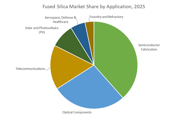
Semiconductor fabrication accounts for approximately 35% of total fused silica demand, positioning it as the largest and most strategically influential end-use segment. This dominance is driven by the extreme operating environment of modern chip manufacturing, where materials must simultaneously tolerate ultra-high temperatures, corrosive plasma chemistries, and zero-defect contamination thresholds. Fused silica is uniquely suited to this role, serving as the backbone material for furnace tubes, wafer carriers, process windows, and plasma chamber components. As device geometries shrink and wafer diameters expand, the tolerance for alkali and metallic impurities has tightened further, making high-purity silica essential for yield protection and process stability. Market share is also reinforced by the scaling of fabrication equipment toward larger wafer formats, which requires massive, dimensionally stable silica components that can maintain uniform properties across large volumes. In plasma-intensive processes, fused silica’s low etch rate directly extends component life, reducing downtime and replacement costs for fabs operating at full capacity. As global semiconductor investment accelerates and advanced-node production expands, semiconductor fabrication remains the core demand engine sustaining fused silica’s market leadership.
The competitive landscape is defined by vertically integrated silica processors, semiconductor-focused optical material leaders, and engineering companies specializing in high-temperature quartzware. Suppliers differentiate through impurity control, homogeneity, refractive index precision, and advanced forming technologies.
Corning remains a global frontrunner in fused silica for lithography systems, offering HPFS® grades engineered for 193 nm and 248 nm laser applications. Its materials feature exceptionally low refractive index variation (AA-grade homogeneity), ensuring accuracy in high-NA projection lenses. Corning’s tight birefringence control (≤1 nm/cm) and certification for inclusion-free substrates position the company as the preferred supplier for semiconductor photonics. Its capacity to produce fused silica blanks up to 450 mm supports advanced photomask and telescope mirror fabrication.
Heraeus Covantics delivers industry-leading purity through its HSQ® and Neonyx® lines, where most impurities fall below detectable limits-ideal for wafer processing and high-performance optics. As a dominant supplier for optical fiber manufacturers, its F300® substrate (OH < 1 ppm) remains the benchmark for core deposition. The company’s wide portfolio spans clear fused quartz to advanced opaque composites for heat shielding. Through refurbishment services for quartzware used in CVD and epitaxy, Heraeus extends equipment lifespan and reduces fab operating costs.
Shin-Etsu Quartz maintains a strong leadership position through decades of innovation in super-high-purity synthetic quartz materials. Its proprietary silicon chemistry and high-precision polishing meet stringent flatness, purity, and durability requirements for semiconductor lithography. The company is also a major supplier of quartz crucibles for silicon crystal pulling-core components of semiconductor-grade wafer production. Its materials exhibit excellent heat resistance and stability in humid cleanroom environments, improving yield in advanced manufacturing processes.
Momentive stands out through its access to premium quartz mines, ensuring a strong supply chain for high-purity silica. Its crucibles offer superior thermal shock resistance for monocrystalline silicon ingot growth, serving both semiconductor and solar industries. The company’s ultra-low OH quartz enables high optical clarity and stability, especially in UV and photonics equipment. High mechanical strength (compressive strength of 1.1×10⁹ Pa) and low-loss dielectric behavior make its materials ideal for next-generation electronics and high-power optical systems.
Nikon differentiates itself through fully in-house production of its NIFS synthetic silica, using direct and soot deposition methods that avoid furnace contamination. This ensures extremely high purity and optical uniformity-vital for ArF and KrF lithography lenses. Advanced annealing techniques yield low birefringence and CTE values near 5.7×10⁻⁷/K, delivering unmatched dimensional stability during high-energy optical exposure. Nikon also supplies silica components for Nd:YAG lasers, astronomy instrumentation, and precision medical devices.
China continues to anchor the global fused silica market by aggressively moving up the value chain from raw quartz processing to high-end synthetic and spherical fused silica products. In 2025, national industrial policy is clearly aligned toward securing domestic access to ultra-high purity (UHP) silica required for advanced semiconductor packaging, 5G infrastructure, and EV electronics. The April 2025 export control announcement by MOFCOM, while framed around rare earths, signaled a broader resource-sovereignty stance that indirectly strengthens domestic fused silica availability for strategic industries.
Industrial clustering has accelerated, particularly around Wuxi’s Functional Materials Industrial Park, where fused silica fillers for epoxy molding compounds (EMCs) are being produced at scale for AI servers and high-frequency electronics. Chinese producers are also responding to thermal management challenges in EV batteries and automotive electronics by expanding spherical fused silica capacity, positioning the country as a cost-competitive yet increasingly quality-focused supplier to global OEMs.
The U.S. fused silica market in 2025 is defined by supply chain resilience and national semiconductor security objectives under the CHIPS and Science Act. Federal funding has catalyzed renewed investment in glass-core substrates, fused silica interposers, and optical-grade wafers that outperform organic laminates in thermal stability for AI accelerators and advanced logic devices. This reshoring push is strategically significant as it reduces exposure to overseas disruptions in high-purity glass materials.
Innovation from domestic players is strengthening the ecosystem, particularly in UV-grade and full-spectrum fused silica wafers required for DUV and EUV lithography. Parallel demand from defense programs-especially high-energy lasers and space-based optical sensors-has reinforced the U.S. position in premium fused silica rods, tubes, and optics, where performance reliability outweighs cost considerations.
Japan remains the undisputed leader in the ultra-high purity end of the fused silica market, maintaining a technological moat built on precision manufacturing and contamination control. In 2025, the country’s role is especially critical for sub-5nm semiconductor nodes, where impurity thresholds fall below parts-per-billion levels. Japanese suppliers continue to dominate synthetic fused silica used in photomasks, EUV components, and advanced glass carriers.
At industry exhibitions and through sustained capital investment, Japanese firms are advancing low-Dk/Df fused silica fillers and ceramic-silica composites that reduce signal loss in emerging 6G and AI computing architectures. This positions Japan not as a volume supplier, but as the global benchmark for performance-critical fused silica applications.
South Korea’s fused silica market growth is tightly coupled with its dominance in High Bandwidth Memory (HBM) and advanced semiconductor packaging. The 2025 capital expenditure surge by memory leaders has translated into soaring demand for fused silica-based epoxy molding compounds and glass substrates capable of withstanding thermal stress in 3D chip stacking.
Packaging innovation has become a national priority, with breakthroughs in through-glass via (TGV) substrates leveraging fused silica’s low thermal expansion to maintain dimensional stability in large AI chips. The rapid establishment of R&D centers focused on quartz crucibles, EUV masks, and advanced substrates underscores South Korea’s intent to internalize critical silica-based inputs for its semiconductor mega-cluster.
Germany functions as Europe’s precision hub for fused silica, balancing optical excellence with energy transition requirements. In 2025, demand has intensified for high-purity fused silica used in photovoltaic crucibles, solar coatings, and optical systems supporting advanced research infrastructure. The country’s clean energy objectives are indirectly strengthening fused silica consumption across renewable manufacturing chains.
German producers are also aligning fused silica production with circular economy principles, piloting recycling of silica feedstock to reduce the energy intensity of electric arc melting. This sustainability-driven innovation is increasingly relevant as European buyers prioritize low-carbon material sourcing without compromising optical or thermal performance.
India is transitioning from a downstream consumer of fused silica to an emerging regional manufacturing hub, driven by its aggressive electronics and semiconductor ambitions. The rapid expansion of smartphone, PCB, and fiber-optic manufacturing in 2025 has created sustained domestic demand for fused silica flour, grains, and fillers used in electronic substrates and high-speed communication infrastructure.
Policy support under the India Semiconductor Mission has expanded to include essential materials, improving the investment climate for domestic fused silica processing. As India scales its 5G rollout and strengthens its position in mobile exports, demand for fused silica preforms and electronic-grade fillers is expected to deepen, anchoring long-term growth in the local market.
|
Country |
Primary Application Focus |
Key Policy / Industry Trigger |
Strategic Material Grade |
|
China |
AI servers & EV electronics |
MOFCOM export controls (Apr 2025) |
Spherical fused silica |
|
United States |
Advanced semiconductor packaging |
CHIPS Act reshoring incentives |
UV-grade fused silica wafers |
|
Japan |
Lithography & 6G electronics |
SEMICON Japan 2025 technology showcase |
Low-Dk/Df synthetic fused silica |
|
South Korea |
HBM & 3D chip stacking |
Semiconductor mega-cluster CapEx surge |
TGV glass substrates |
|
Germany |
Solar PV & optical systems |
Renewable energy and circular economy mandates |
UHP synthetic quartz |
|
India |
Consumer electronics & 5G |
India Semiconductor Mission expansion |
Fused silica flour and grains |
|
Parameter |
Details |
|
Market Size (2025) |
$2.6 Billion |
|
Market Size (2035) |
$4.6 Billion |
|
Market Growth Rate |
5.8% |
|
Segments |
By Purity Level (Ultrapure Synthetic Fused Silica, High Purity Fused Silica, Standard Purity Fused Silica), By Product Form (Grains & Granules, Flour & Powder, Ingots & Blocks, Rods & Tubes, Plates & Disks), By Application (Semiconductor Fabrication, Optical Components, Telecommunications, Solar & Photovoltaics, Foundry & Refractory, Aerospace & Defense, Healthcare & Life Sciences), By End-User Industry (Electronics & Microelectronics, Energy & Power, Industrial Manufacturing, Aerospace & Defense, Sciences & Research) |
|
Study Period |
2019- 2024 and 2025-2034 |
|
Units |
Revenue (USD) |
|
Qualitative Analysis |
Porter’s Five Forces, SWOT Profile, Market Share, Scenario Forecasts, Market Ecosystem, Company Ranking, Market Dynamics, Industry Benchmarking |
|
Companies |
Corning Incorporated, Heraeus Covantics, Shin-Etsu Chemical Co., Ltd., Tosoh Corporation, Momentive Performance Materials Inc., SCHOTT AG, Evonik Industries AG, Feilihua Quartz Glass Co., Ltd., Jiangsu Pacific Quartz Co., Ltd., Saint-Gobain S.A., Nikon Corporation, AGC Inc., CoorsTek Inc., U.S. Silica Holdings Inc., Ferro Corporation |
|
Countries |
US, Canada, Mexico, Germany, France, Spain, Italy, UK, Russia, China, India, Japan, South Korea, Australia, South East Asia, Brazil, Argentina, Middle East, Africa |
*- List not Exhaustive
Table of Contents: Fused Silica Market
1. Executive Summary
1.1. Market Highlights
1.2. Key Findings
1.3. Global Market Snapshot
2. Fused Silica Market Landscape & Outlook (2025–2034)
2.1. Introduction to Fused Silica Market
2.2. Market Valuation and Growth Projections (2025–2034)
2.3. Yield Sensitivity and Material Criticality in Semiconductor Manufacturing
2.4. Impurity Control, Thermal Stability, and Optical Homogeneity Requirements
2.5. Supply Chain Integration, Qualification Cycles, and Traceability
3. Innovations Reshaping the Fused Silica Market
3.1. Trend: Low-β Fused Silica for High-NA EUV Lithography
3.2. Trend: Large-Aperture Monolithic Fused Silica for Space and Physics Applications
3.3. Opportunity: Synthetic Fused Silica Crucibles for Onshored CZ Silicon Manufacturing
3.4. Opportunity: Radiation-Hardened Fused Silica Fibers for Nuclear and Space Systems
4. Competitive Landscape and Strategic Initiatives
4.1. Mergers and Acquisitions
4.2. R&D and Ultra-High-Purity Material Innovation
4.3. Sustainability, Circular Quartz Processing, and ESG Strategies
4.4. Capacity Expansion and Regional Manufacturing Focus
5. Market Share and Segmentation Insights: Fused Silica Market
5.1. By Purity Level
5.1.1. Ultrapure Synthetic Fused Silica
5.1.2. High Purity Fused Silica
5.1.3. Standard Purity Fused Silica
5.2. By Product Form
5.2.1. Grains and Granules
5.2.2. Flour and Powder
5.2.3. Ingots and Blocks
5.2.4. Rods and Tubes
5.2.5. Plates and Disks
5.3. By Application
5.3.1. Semiconductor Fabrication
5.3.2. Optical Components
5.3.3. Telecommunications
5.3.4. Solar and Photovoltaics
5.3.5. Foundry and Refractory
5.3.6. Aerospace and Defense
5.3.7. Healthcare and Life Sciences
6. Country Analysis and Outlook of Fused Silica Market
6.1. United States
6.2. Canada
6.3. Mexico
6.4. Germany
6.5. France
6.6. Spain
6.7. Italy
6.8. United Kingdom
6.9. Russia
6.10. China
6.11. India
6.12. Japan
6.13. South Korea
6.14. Australia
6.15. South East Asia
6.16. Brazil
6.17. Argentina
6.18. Middle East
6.19. Africa
7. Fused Silica Market Size Outlook by Region (2025–2034)
7.1. North America Fused Silica Market Size Outlook to 2034
7.1.1. By Purity Level
7.1.2. By Product Form
7.1.3. By Application
7.1.4. By Country
7.2. Europe Fused Silica Market Size Outlook to 2034
7.2.1. By Purity Level
7.2.2. By Product Form
7.2.3. By Application
7.2.4. By Country
7.3. Asia Pacific Fused Silica Market Size Outlook to 2034
7.3.1. By Purity Level
7.3.2. By Product Form
7.3.3. By Application
7.3.4. By Country
7.4. South America Fused Silica Market Size Outlook to 2034
7.4.1. By Purity Level
7.4.2. By Product Form
7.4.3. By Application
7.4.4. By Country
7.5. Middle East and Africa Fused Silica Market Size Outlook to 2034
7.5.1. By Purity Level
7.5.2. By Product Form
7.5.3. By Application
7.5.4. By Country
8. Company Profiles: Leading Players in the Fused Silica Market
8.1. Corning Incorporated
8.2. Heraeus Covantics
8.3. Shin-Etsu Chemical Co., Ltd.
8.4. Tosoh Corporation
8.5. Momentive Performance Materials Inc.
8.6. SCHOTT AG
8.7. Evonik Industries AG
8.8. Feilihua Quartz Glass Co., Ltd.
8.9. Jiangsu Pacific Quartz Co., Ltd.
8.10. Saint-Gobain S.A.
8.11. Nikon Corporation
8.12. AGC Inc.
8.13. CoorsTek, Inc.
8.14. U.S. Silica Holdings, Inc.
8.15. Ferro Corporation
9. Methodology
9.1. Research Scope
9.2. Market Research Approach
9.3. Market Sizing and Forecasting Model
9.4. Research Coverage
9.5. Data Horizon
9.6. Deliverables
10. Appendix
10.1. Acronyms and Abbreviations
10.2. List of Tables
10.3. List of Figures
The global Fused Silica Market was valued at USD 2.6 billion in 2025 and is forecast to reach USD 4.6 billion by 2035, registering a CAGR of 5.8% during 2026–2035. Growth is anchored in semiconductor fabrication, EUV lithography, and high-stability optical systems where material reliability directly impacts yield and uptime.
As chipmakers scale below 5 nm and deploy High-NA EUV systems, fused silica has shifted from a passive substrate to a yield-critical material. Ultra-low impurity levels, near-zero thermal expansion, and refractive index homogeneity are essential to control overlay error, thermal drift, and wavefront distortion in high-energy lithography environments.
Ultrapure synthetic fused silica accounts for the largest value share, driven by its irreplaceable role in photomasks, wafer processing, and laser optics. Its ppb-level impurity control, superior homogeneity, and resistance to laser-induced damage make it the preferred choice despite higher material costs, as it protects downstream yield and tool lifetime.
Beyond lithography, growth is accelerating in synthetic fused silica crucibles for onshored semiconductor wafer production, radiation-hardened fibers for nuclear and space applications, and large-aperture monolithic optics for space telescopes and fundamental physics. These applications demand extreme thermal stability, low birefringence, and long-term dimensional predictability.
Leading players include Corning Incorporated, Heraeus Covantics, Shin-Etsu Chemical, Tosoh Corporation, Momentive Performance Materials, SCHOTT AG, Nikon Corporation, AGC Inc., Saint-Gobain, and Feilihua Quartz Glass. Market leaders differentiate through ultra-high purity synthesis, semiconductor-qualified grading, large-format capability, and long-term supply reliability.