Market Overview: Glass Substrate Market Size, Growth Outlook, and Key Industry Insights
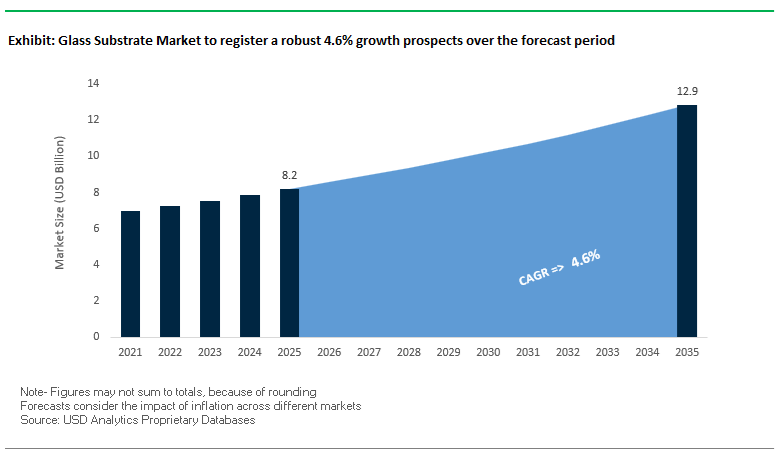
The Glass Substrate Market, valued at USD 8.2 billion in 2025, is projected to reach USD 12.9 billion by 2035, expanding at a CAGR of 4.6% (2025–2035). The demand trajectory is being shaped by rapid advancements in semiconductor packaging, consumer electronics, and high-frequency communication infrastructure. Manufacturers and vendors are increasingly transitioning toward ultra-thin, alkali-free glass, high-density Through-Glass Via (TGV) architectures, and large-format substrates capable of sustaining advanced lithographic processes. With AI accelerators, HPC chipsets, foldable displays, and 5G/6G hardware accelerating their adoption curves, glass substrates are becoming a mission-critical material enabling next-generation device miniaturization and signal integrity.
Industry data reveals that sub-2µm RDL line/space geometries are now being demonstrated for high-density chiplet integration, marking a transformative step for AI, RF, and logic packaging supply chains. Additionally, breakthroughs in Laser-Induced Deep Etching (LIDE) have resulted in TGV aspect ratios surpassing 15:1, significantly enhancing vertical interconnection efficiencies. Vendors are also leveraging the dimensional stability advantages of glass—achieving less than 20 µm warpage on 100 mm formats—to meet lithography alignment tolerances that organic substrates cannot achieve. In parallel, the material’s ultra-low dielectric loss is enabling mission-critical performance for applications spanning 100–300 GHz mmWave, RF front-end modules, and Massive MIMO hardware. The consumer electronics ecosystem is pushing the boundary further, with manufacturers targeting sub-100 µm chemically strengthened glass for next-generation foldable and ultra-thin devices.
Key Industry Insights
- Sub-2 µm RDL geometries reinforce glass as a core enabler for advanced chip packaging and AI accelerator architectures.
- LIDE-processed TGVs exceeding 15:1 aspect ratios unlock high-density vertical interconnects for semiconductor scaling.
- Glass substrates exhibit exceptional dimensional stability (<20 µm warpage), supporting advanced lithography and panel-level packaging.
- Low-loss performance extends suitability to 100–300 GHz 5G/6G mmWave systems, RF modules, and high-frequency communication chips.
- Premium electronics manufacturers are advancing <100 µm ultra-thin, alkali-free substrates for flexible and foldable devices.
Market Analysis: Expansion Strategies, Technology Shifts, and Policy-Driven Investments in the Glass Substrate Industry
The global Glass Substrate Market is undergoing rapid transformation due to technological breakthroughs and capacity expansions across display, semiconductor, and solar value chains. In May 2023, Corning Incorporated announced a 20% price increase for its display glass substrates—an important signal of tightening supply, rising input costs, and strategic margin recovery for large-area substrate formats such as Gen 10.5 glass used in premium televisions. The same year, in September 2023, SCHOTT AG released a focused, three-point action plan to accelerate its presence in semiconductor packaging, highlighting the industry’s pivot toward glass-core substrates, carrier wafers, and fine-pitch interposers.
The solar and renewable energy segment also recorded notable developments. In November 2023, NSG Group announced a major investment in expanding Transparent Conductive Oxide (TCO) glass manufacturing capacity in the United States, addressing surging domestic demand driven by clean-energy incentives and reshoring policies. Meanwhile, Corning expanded its premium electronics material portfolio with the launch of Eagle XG NEXT ultrathin glass in November 2023, targeting foldable displays and high-end mobile devices. The competitive landscape shifted further when SCHOTT acquired a display glass plant in Korea in February 2024, strengthening its supply footprint in Asia’s mature display manufacturing ecosystem.
Sustainability and next-gen semiconductor packaging are emerging as dominant themes. In February 2023, AGC Inc. and Saint-Gobain jointly initiated a breakthrough pilot project to design a low-carbon flat glass production line aimed at sharply reducing process CO₂ emissions—demonstrating the sector’s movement toward greener manufacturing. The momentum for advanced packaging materials continued into April 2025, when LPKF and Onto Innovation formalized a collaboration to accelerate mass production of glass-core substrates using LIDE-enabled TGV architectures. Regional diversification also intensified, with 3D Glass Solutions (3DGS) gaining Indian government approval in 2025 to establish an advanced packaging unit in Odisha targeting 3D heterogeneous integration. A defining milestone for the industry came when Intel, in late 2024, outlined its roadmap for transitioning from organic to glass substrates for next-generation high-bandwidth packages, signaling long-term endorsement from one of the world’s largest semiconductor manufacturers.
Key Trends Driving High-Volume Adoption of Glass Substrates in AI and HPC Packaging
Market Trend 1: Rapid Acceleration of Glass Substrate Integration for AI and High-Performance Computing
The semiconductor industry is witnessing a pivotal shift as glass core substrates emerge as critical enablers for next-generation AI and HPC packaging architectures. Public corporate roadmaps—most notably from Intel—demonstrate explicit alignment toward glass-based substrate adoption for post-2026/2027 high-volume manufacturing (HVM). This clarity of commercialization intent marks a significant maturation point for the global glass substrate ecosystem.
In addition to roadmap visibility, glass substrates offer a transformative leap in integration density, with research prototypes supporting the mounting of up to 60 chips within a single multi-die package, far exceeding the physical limits of conventional organic or silicon substrates. Such density advancement is crucial to scaling AI accelerators, GPU complexes, and chiplet-based architectures that require massive I/O bandwidth and increasingly complex interconnect topologies.
The trend is further validated by a surge in patent filings from major semiconductor innovators including Intel, Huawei, and multiple OSATs, with notable intellectual property concentration in glass interposers, through-glass vias (TGV) formation, glass-based hybrid bonding, and fine-line RDL patterning. The aggressive patent race signals a strong competitive push to secure technical leadership in glass substrate technologies, positioning this material class as a strategic innovation platform for the next decade of heterogeneous integration.
Market Trend 2: Government-Backed Investments Strengthening Domestic Advanced Packaging Infrastructure
Government intervention is rapidly emerging as a decisive force accelerating commercialization and supply chain readiness for glass-based advanced packaging. The U.S. CHIPS and Science Act—particularly through the National Advanced Packaging Manufacturing Program (NAPMP)—has allocated over $1.4 billion to strengthen domestic packaging capabilities. This includes dedicated investment streams to develop technologies that directly support the maturation of glass substrate manufacturing, metrology, and process integration.
A landmark milestone in this trend is the $100 million award to Absolics, Inc., designed to catalyze a robust glass-core packaging ecosystem in the United States. This targeted funding demonstrates policy recognition of glass substrates as a national priority for semiconductor competitiveness, particularly in AI hardware and HPC infrastructure.
Further reinforcing this direction, government-backed facilities such as the Natcast Advanced Packaging Piloting Facility (PPF) are mandated to bridge R&D and volume manufacturing. These facilities include capabilities for TGV drilling, glass-based interposers, hybrid bonding, thermal-mechanical simulation, and other processes essential to maturing glass into a commercially scalable substrate platform. Collectively, these initiatives propel the U.S.—and partner regions—toward leadership in the global glass substrate market.
Strategic Opportunities Supporting Wider Industry Adoption of Glass Substrates
Market Opportunity 1: Unlocking Power Efficiency and Thermal Stability for Next-Generation Chip Architectures
Glass substrates unlock significant opportunities to improve power efficiency, signal integrity, and thermal performance, three constraints that increasingly limit scaling of AI accelerators and HPC processors. One of the most compelling attributes is glass’s ultra-low Coefficient of Thermal Expansion (CTE), as low as 3 ppm/°C, which nearly matches silicon. This thermal compatibility reduces warpage by up to 50%, mitigating die stress and improving long-term package reliability—an essential requirement as die sizes increase and chiplet architectures become more thermally demanding.
Beyond mechanical stability, glass provides superior electrical performance, with a dielectric constant (Dk ≈ 2.8) significantly lower than silicon or organic cores. Combined with low tangent loss, this results in exceptionally low high-frequency transmission losses, supporting 15–20% power reduction for high-speed interconnects critical to AI fabrics, HBM stacks, and next-gen PCIe/CXL links.
Glass substrates also enable sub-2 μm line/space Redistribution Layer (RDL) patterning—a threshold organic substrates struggle to reach. This capability directly supports higher I/O density, chiplet integration, 3D packaging, and the ultra-dense interconnects required for future multi-tile GPU/AI processors. For semiconductor designers, the materials opportunity translates into greater bandwidth, reduced latency, and more scalable system architectures.
Market Opportunity 2: Standardization and Ecosystem Building for Mid-Tier Foundry and OSAT Customers
A major opportunity lies in developing a scalable, standardized ecosystem for panel-level packaging (PLP) using glass substrates. Glass is inherently well-suited to large-format panels (e.g., 500 mm x 500 mm), enabling cost-efficient batch manufacturing and leveraging legacy display industry infrastructure, which significantly reduces capital expenditure. As PLP adoption increases, mid-tier foundries and OSATs gain access to high-end packaging capabilities previously limited to top-tier IDMs.
Industry collaboration is accelerating this transition. Partnerships between equipment manufacturers (such as LPKF and Onto Innovation) and research institutes like Fraunhofer IZM are defining standardized process flows for glass core substrate manufacturing, including TGV formation, laser drilling, RDL processing, and defect inspection. These standardization efforts de-risk adoption and shorten time-to-market for customers entering advanced packaging segments.
Furthermore, the integration of standardized features such as TGVs and embedded silicon bridges transforms glass into a modular platform enabling pre-defined interposer architectures. Mid-tier foundry customers can adopt these platforms without bearing the full R&D cost of custom interposer design, opening new opportunities for heterogeneous integration, chiplet ecosystems, and high-performance packaging solutions.
Glass Substrate Market Share Analysis
Market Share by Type: Dominance of Borosilicate Glass Substrates in High-Performance Applications
Borosilicate glass substrates hold the largest share—approximately 25% of the global glass substrate market—due to their superior material characteristics and their essential role in precision-driven, high-temperature manufacturing environments. Their low coefficient of thermal expansion, high thermal stability, and strong resistance to chemical degradation make them indispensable in advanced display technologies, photovoltaic modules, and semiconductor wafer processing. This dominance is further strengthened by the rapid expansion of OLED and LCD display production, where optical clarity, temperature endurance, and surface uniformity directly influence device performance and yield rates. As manufacturers push toward ultra-thin, lightweight, and high-durability display formats, borosilicate substrates continue to outperform alternatives, securing their leadership position. In solar applications, their stability under fluctuating climatic conditions enhances module lifespan, contributing to higher adoption in utility-scale and rooftop installations. The growing focus on next-generation microelectronics, including AI and HPC chip architectures, further elevates the segment’s importance, as borosilicate substrates offer reliable dielectric properties essential for fine-line lithography and advanced packaging—strengthening their overall market share across high-value, innovation-driven sectors.
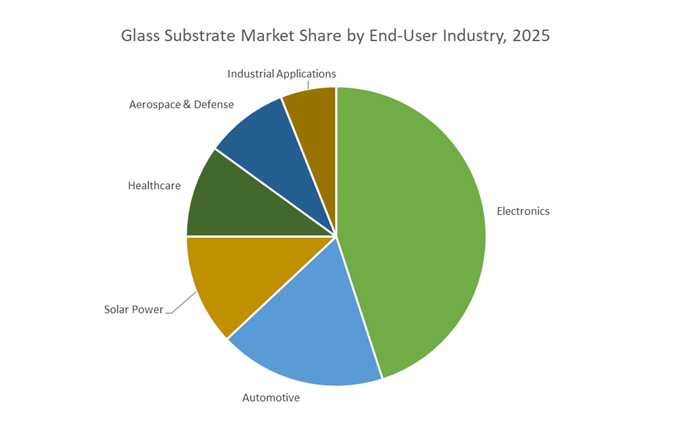
Market Share by End-User Industry: Electronics Sector as the Primary Demand Engine
The electronics industry leads the market with ~45% share, reflecting its central role in global manufacturing ecosystems where glass substrates are critical enablers of technological advancement. This dominance is rooted in surging demand for high-resolution displays, semiconductor devices, and ultra-thin, durable materials required for modern consumer electronics. Smartphones, tablets, OLED TVs, digital signage, and next-generation laptops rely heavily on precision-engineered glass substrates that support superior optical performance, structural rigidity, and heat resistance during device fabrication. The rise of foldable and flexible electronics is also accelerating the shift toward advanced glass compositions capable of maintaining mechanical integrity while enabling sleek designs. Additionally, semiconductor innovations—particularly in AI accelerators, 5G chipsets, and 2.5D/3D integrated packaging—are reshaping substrate requirements, with glass increasingly replacing organic materials due to its inherent dimensional stability and excellent electrical insulation. Wearable electronics, smart appliances, and IoT ecosystems further amplify demand, as each device requires miniaturized, robust, and thermally efficient display and sensor components. Together, these dynamics reinforce the electronics sector as the dominant consumer of glass substrates and position it as the highest-growth contributor to future market expansion.
Country Analysis: Hotspots for Glass Substrate Innovation
South Korea: Advanced Semiconductor Packaging Leadership and Glass Core Substrate Commercialization
South Korea stands at the forefront of high-performance glass substrate innovation, emerging as one of the most strategically influential regions in the global Glass Substrate Market. The country’s dominance is anchored in its aggressive semiconductor roadmap, rapid scaling of advanced packaging technologies, and the presence of global electronics powerhouses that continually elevate substrate performance benchmarks. A major boost has come from SKC’s accelerated Glass Core Substrate (GCS) commercialization strategy, supported by the development of its U.S.-based Absolics facility—a $240 million advanced IC packaging plant in Georgia that strengthens South Korea’s global GCS footprint. Samsung Electro-Mechanics (Semco) is also intensifying its R&D around next-generation substrates, targeting unprecedented wiring density and superior thermal behavior required for AI processors and high-performance computing architectures. This is further reinforced by the South Korean government’s multi-trillion-won semiconductor support program, heavily concentrated in the Yongin Cluster, attracting upstream glass substrate material suppliers, tooling manufacturers, and packaging ecosystem innovators.
R&D activity across the region is equally robust, as companies like LG Innotek pursue miniaturization breakthroughs using glass substrates for ultra-dense thin-film packaging, RF-MEMS modules, and compact optical units such as advanced camera systems. South Korea’s leadership is also reinforced by the regional expansion of SCHOTT AG’s AR waveguide supply chain, driven by Lumus' Z-Lens technology, which enhances AR display manufacturing precision. Collectively, these advancements position Korea as a global nucleus for semiconductor-grade glass substrates, GCS innovation, and next-generation heterogeneous integration solutions.
China: Ultra-Thin Display Leadership and Intensified Domestic Semiconductor Substrate Investment
China’s influence on the Glass Substrate Market continues to expand rapidly, driven by massive capacity additions in display technology, photovoltaic module manufacturing, and domestic semiconductor ecosystem development. The country’s leadership in ultra-thin display glass was reinforced when BOE unveiled a P0.9 small LED display on a glass substrate, showcasing superior pixel density, reduced energy consumption, and enhanced mechanical stability—critical factors for next-generation TVs, AR/VR systems, and signage displays. Simultaneously, China’s state-backed semiconductor investment programs, including allocations from the Big Fund, are directly enhancing domestic substrate production capabilities. Billions are being channelled into localizing the IC packaging value chain, with special attention on developing glass-based packaging platforms to reduce reliance on foreign suppliers.
In parallel, China’s dominance in solar photovoltaic manufacturing remains unmatched, powered by extensive float glass and low-iron solar glass production essential for large-scale solar module output. Local companies are also piloting advanced GCS lines to support 5G infrastructure, data center interconnects, and chiplet-based computing systems, where higher bandwidth and lower signal loss are critical. These combined advancements solidify China’s position as a dual-driven hotspot—leading in high-volume display glass and rapidly strengthening its semiconductor substrate capabilities.
United States: Strategic Investments in TGV Interposers and Semiconductor-Grade Glass Substrates
The United States is accelerating its capabilities in advanced packaging and semiconductor-grade glass substrates, fuelled significantly by the CHIPS and Science Act, which continues to catalyze domestic manufacturing investments. One of the most notable developments is Absolics’ construction of a GCS production facility in Georgia, expected to initiate production in 2025 and play a foundational role in reshoring substrate supply for AI chips, HPC processors, and high-density interposers. In parallel, Corning’s global price increase for display glass substrates is a strategic realignment aimed at countering escalating raw materials and energy costs—ultimately stabilizing U.S. supply chain reliability while reinforcing Corning’s leadership in high-generation display glass technologies.
The U.S. is also witnessing substantial innovation in IC substrates, as demonstrated by KLA’s 2024 introduction of advanced imaging and metrology systems optimized for precision panel-based interconnects and glass substrate manufacturing. The defense and aerospace sectors amplify this momentum, leveraging fused silica and quartz glass substrates for RF systems, MEMS devices, and mission-critical electronics where thermal stability and dielectric performance are paramount. Together, these developments underscore the U.S.’s transition into a high-value hub for TGV interposers, GCS manufacturing, and next-generation semiconductor substrate engineering.
Japan: Precision Optical Glass Manufacturing and Strategic Semiconductor Material Upgrades
Japan continues to be a global benchmark for precision glass engineering, maintaining leading positions across optical substrates, high-generation display glass, and semiconductor material innovation. Companies such as Nippon Electric Glass (NEG) and Hoya Corporation dominate the production of ultra-flat LCD and OLED substrates, offering unparalleled surface quality and reliability demanded by premium consumer electronics and industrial displays. Simultaneously, AGC’s attainment of an Environmental Product Declaration (EPD) for its architectural float glass reflects growing alignment with global sustainability goals, signalling Japan’s continued leadership in eco-certified, high-integrity material manufacturing.
Japan’s semiconductor resurgence—driven by government investments exceeding ¥10 trillion—has reinvigorated its local materials landscape. Through consortia including Rapidus, significant funding now targets next-generation glass substrates, photolithography masks, and advanced optics vital for EUV lithography. Ohara Inc. strengthens this ecosystem with its expertise in high-homogeneity optical glass substrates used in photonics, LiDAR, high-end imaging optics, and photonic integrated circuits (PICs). Japan’s precision-driven manufacturing capabilities and its renewed semiconductor push collectively anchor it as a premium supplier of ultra-specialized glass substrate technologies.
Germany: Specialty Glass Engineering for ADAS, MEMS, and High-Reliability Electronics
Germany remains a key innovation center for specialty glass substrates, supported by its strong automotive and industrial electronics sectors. Companies like SCHOTT AG play a pivotal role in developing advanced glass substrates for ADAS and LiDAR systems, where thermal resilience, surface durability, and optical clarity are mission-critical. SCHOTT’s continued expansion into smart kitchen technologies, such as CERAN Luminoir and CleanPlus coatings, demonstrates how specialty technical glass is also moving into premium consumer appliance ecosystems, widening the substrate application base.
The German government, through BMWK, is accelerating localized IC packaging R&D, enabling the emergence of glass-reinforced substrates targeted at power modules, radar electronics, and high-frequency automotive systems. In addition, Plan Optik AG continues to lead the European market in TGV processing and high-precision glass wafer fabrication, supplying MEMS, microfluidics, and semiconductor packaging firms with custom-engineered substrate solutions. Germany’s role as a precision-focused technical glass hub ensures sustained demand for high-reliability substrate materials tailored to mission-critical electronics.
India: Rise of Domestic Semiconductor Packaging and Glass Interposer Manufacturing
India is fast emerging as a competitive growth market for glass substrates, propelled by government-led semiconductor incentives and large-scale electronics manufacturing programs. The India Semiconductor Mission (ISM) approved four new semiconductor projects in 2025, including a cutting-edge facility by 3D Glass Solutions Inc. focused on glass interposers, silicon bridges, and 3D heterogeneous integration modules. This represents a transformational shift, positioning India as a future supplier of advanced glass-based packaging solutions used in AI accelerators, RF modules, and miniaturized computing devices.
The Production-Linked Incentive (PLI) scheme continues to attract global display and electronic component manufacturers to establish local assembly and fabrication units, significantly lifting domestic demand for OLED glass, touchscreen glass, and mobile display substrates. The solar sector also boosts consumption of photovoltaic (PV) glass substrates, supported by India’s multi-GW solar installation pipeline. Together, these initiatives create a favorable ecosystem for glass substrate expansion, combining semiconductor innovation with large-scale manufacturing momentum.
Competitive Landscape: Leading Glass Substrate Manufacturers and Their Strategic Positions
The competitive environment in the Global Glass Substrate Market is shaped by deep manufacturing expertise, proprietary process technologies, and strategic expansions across semiconductor, display, and solar verticals. Companies are increasingly investing in nanoscale precision, low-carbon production, and advanced packaging capabilities to align with high-growth application areas such as AI processors, foldable displays, mmWave communications, and PV infrastructure. The competitive edge is largely derived from innovation pipelines, geographical scaling, and the ability to supply ultra-thin, defect-free substrates at high volumes.
Corning Incorporated: Advancing Ultra-Thin and High-Purity Glass Technologies
Corning continues to set the benchmark in specialty glass manufacturing through its fusion-forming process, enabling exceptionally smooth, ultra-flat substrates essential for next-generation display backplanes and semiconductor applications. Its portfolio, including EAGLE XG glass, remains central to TFT-LCD and OLED production lines worldwide. The company’s strategic emphasis on optical and ceramic innovations strengthens its leadership in emerging areas such as co-packaged optics and glass-based semiconductor packaging. The launch of Eagle XG NEXT in November 2023 reflects Corning’s intent to dominate the foldable and rollable device substrate market, reinforcing its position at the forefront of high-performance material design.
AGC Inc.: Expanding Energy-Efficient and High-Performance Glass Substrate Capabilities
AGC maintains a diversified and technologically advanced product ecosystem that spans display glass, borosilicate materials, and thin specialty glass for electronics. Its application leadership extends to automotive displays and HUD systems, where durability and optical clarity are critical differentiators. A defining advantage for AGC is its Digital Twin–enabled CADTANK optimization technology, deployed (Jan 2023) to enhance glass melting efficiency and yield. AGC’s collaboration with Saint-Gobain in February 2023 to develop a low-carbon pilot manufacturing line underscores its strategic commitment to decarbonization and future regulatory alignment.
SCHOTT AG: Strengthening Glass Solutions for Advanced Semiconductor Packaging
SCHOTT is deeply positioned in high-precision, high-value substrate categories through offerings such as FLEXINITY connect, introduced in January 2022 to support miniaturized semiconductor packaging. Its portfolio encompasses fused silica, quartz, and borosilicate glass, catering to optical, semiconductor, and scientific applications. In September 2023, SCHOTT announced a strategic roadmap to scale its contribution to glass-based interposers and TGV-enabled packaging, addressing the surge in HPC and AI processing workloads. The company’s acquisition of a Korean display plant in February 2024 further solidifies its capacity to serve global demand.
Nippon Sheet Glass (NSG Group): Scaling TCO and Electronics Glass for Renewable Energy Growth
NSG Group is a central supplier of Transparent Conductive Oxide (TCO) Glass, crucial for thin-film solar modules and large-scale PV installations. It also manufactures thin, strengthened substrates for mobile and display backplanes. The company’s November 2023 US expansion plan marks a strategic shift to increase its North American footprint amid rising solar deployment and policy-driven demand. NSG's internal R&D capacity, bolstered by the establishment of its Second Research Building in December 2022, enables continuous advancements in processing technologies for electronics-grade glass.
HOYA Corporation: Precision Glass for Lithography and High-Density Data Storage
HOYA maintains a strong leadership position in ultra-low thermal expansion glass substrates used in semiconductor lithography masks—an essential component for shrinking integrated circuit geometries. Its high-precision polishing techniques deliver nanoscale flatness, supporting both EUV lithography and high-density hard disk drive technologies. HOYA’s contributions to the semiconductor ecosystem extend into optical, data storage, and precision imaging markets, where material purity and dimensional stability are critical. Its glass HDD substrates are increasingly preferred over aluminum due to superior shock resistance and stability, enabling higher data densities for cloud and enterprise storage.
Glass Substrate Market Report Scope
Glass Substrate Market
|
Parameter
|
Details
|
|
Market Size (2025)
|
$8.2 Billion
|
|
Market Size (2035)
|
$12.9 Billion
|
|
Market Growth Rate
|
4.6%
|
|
Segments
|
By Type (Borosilicate Glass Substrates, Fused Silica/Quartz Glass Substrates, Silicon-Based Glass Substrates, Ceramic Glass Substrates, Alkali-Free Glass Substrates, Other Glass Ceramics), By Wafer Diameter (Up to 100 mm, 125 mm, 150 mm, 200 mm, 300 mm, Above 300 mm), By Application (Wafer-Level Packaging, Substrate Carriers, TGV Interposers, Flat Panel Displays, Optics & Photonics Components, MEMS & CMOS Image Sensors, Hard Disk Drives), By End-User Industry (Electronics, Automotive, Solar Power, Healthcare, Aerospace & Defense, Industrial Applications)
|
|
Study Period
|
2019- 2024 and 2025-2034
|
|
Units
|
Revenue (USD)
|
|
Qualitative Analysis
|
Porter’s Five Forces, SWOT Profile, Market Share, Scenario Forecasts, Market Ecosystem, Company Ranking, Market Dynamics, Industry Benchmarking
|
|
Companies
|
Corning Incorporated, AGC Inc., Nippon Electric Glass, SCHOTT AG, Hoya Corporation, Saint-Gobain, SKC/Absolics, Ohara Inc., Plan Optik AG, Samsung Electro-Mechanics, LG Innotek, AvanStrate, Nippon Sheet Glass, Hoya Candeo Optronics, Toppan Inc.
|
|
Countries
|
US, Canada, Mexico, Germany, France, Spain, Italy, UK, Russia, China, India, Japan, South Korea, Australia, South East Asia, Brazil, Argentina, Middle East, Africa
|
Glass Substrate Market Segmentation
By Type
- Borosilicate Glass Substrates
- Fused Silica / Quartz Glass Substrates
- Silicon-Based Glass Substrates
- Ceramic Glass Substrates
- Alkali-Free Glass Substrates
- Other Glass Ceramics
By Wafer Diameter
- Up to 100 mm
- 125 mm
- 150 mm (6-inch)
- 200 mm (8-inch)
- 300 mm (12-inch)
- Above 300 mm
By Application
- Wafer-Level Packaging (WLP)
- Substrate Carriers
- TGV Interposers
- Flat Panel Displays
- Optics and Photonics Components
- MEMS and CMOS Image Sensors
- Hard Disk Drives
By End-User Industry
- Electronics
- Automotive
- Solar Power
- Healthcare
- Aerospace and Defense
- Industrial Applications
By Region
- North America (United States, Canada, Mexico)
- Europe (Germany, France, United Kingdom, Spain, Italy, Rest of Europe)
- Asia Pacific (China, India, Japan, South Korea, Australia, Rest of APAC)
- South and Central America (Brazil, Argentina, Rest of SCA)
- Middle East and Africa (Saudi Arabia, UAE, South Africa, Rest of Middle East, Rest of Africa)
Top Companies in Glass Substrate Market
- Corning Incorporated (USA)
- AGC Inc. (Japan)
- Nippon Electric Glass (Japan)
- SCHOTT AG (Germany)
- Hoya Corporation (Japan)
- Saint-Gobain (France)
- SKC/Absolics (South Korea)
- Ohara Inc. (Japan)
- Plan Optik AG (Germany)
- Samsung Electro-Mechanics (South Korea)
- LG Innotek (South Korea)
- AvanStrate (Japan/India)
- Nippon Sheet Glass (Japan)
- Hoya Candeo Optronics (Japan)
- Toppan Inc. (Japan)
*- List not Exhaustive
Research Coverage
This report investigates the rapidly evolving Glass Substrate Market, delivering an authoritative review of breakthroughs, technology shifts, manufacturing innovations, and competitive dynamics shaping the global landscape. Developed by USDAnalytics, the analysis reviews the transformative impact of glass-core substrates, high-density TGV architectures, ultra-thin display materials, and semiconductor-grade glass innovations on major electronics, renewable energy, and advanced packaging value chains. The study highlights the accelerating integration of glass substrates in AI accelerators, HPC chipsets, 5G/6G communications, and next-generation display ecosystems, offering a deep dive into policy-led investments, ecosystem maturity, and strategic capacity expansions across leading regions. This report is an essential resource for industry professionals, investors, and technology stakeholders seeking fact-driven insights, granular segmentation, and forward-looking assessments that map the market’s evolution from 2021 through 2034.
Scope Highlights
- Segmentation: Comprehensive analysis by Type (Borosilicate, Fused Silica/Quartz, Silicon-Based, Ceramic Glass, Alkali-Free, Other Glass Ceramics), Wafer Diameter (≤100 mm to Above 300 mm), Application (WLP, Substrate Carriers, TGV Interposers, Displays, Optics/Photonics, MEMS, HDDs), and End-User (Electronics, Automotive, Solar, Healthcare, Aerospace & Defense, Industrial).
- Geographic Scope: Coverage includes 25+ countries across North America, Europe, Asia Pacific, Latin America, and the Middle East & Africa.
- Timeframe: Market modeling includes historic data (2021–2024) and forecast projections (2025–2034) for transparent and robust strategic planning.
- Companies: Includes competitive assessments and profile reviews of 15+ leading manufacturers shaping the global glass substrate value chain.
