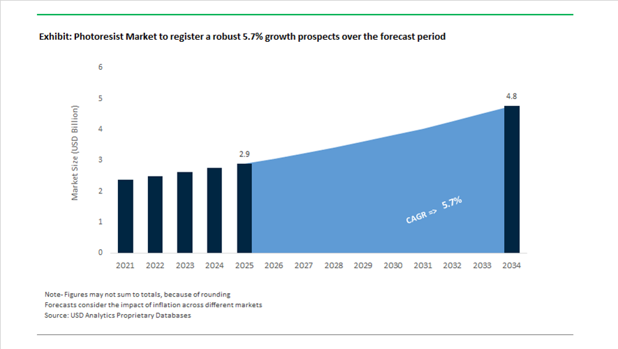
Photoresist Market Size 2025–2034: $2.9 Billion to $4.8 Billion at 5.7% CAGR Accelerated by High-NA EUV, AI Chips, and Advanced Packaging
The global photoresist market is projected to expand from $2.9 billion in 2025 to $4.8 billion by 2034, registering a CAGR of 5.7%. Growth in the EUV photoresist market, ArF immersion resists, KrF resists, and dry film photoresists is being driven by rapid scaling of generative AI processors, High-Bandwidth Memory (HBM3e and HBM4), advanced packaging, and sub-2nm semiconductor nodes. As chip geometries shrink and 3D architectures proliferate, demand for high-sensitivity, low line-edge roughness (LER), and high-etch-resistance photoresist materials is intensifying. The transition toward High-NA EUV lithography represents the most significant structural shift in the semiconductor photoresist industry in over a decade.
Japan strengthened its leadership in advanced lithography materials through strategic restructuring in 2024. In June 2024, Japan Investment Corporation completed its $6.4 billion acquisition of JSR Corporation, with full delisting finalized in December 2024. This move enables long-term R&D investment in next-generation EUV photoresists and consolidates national semiconductor materials capabilities. In April 2024, Shin-Etsu Chemical committed ¥83 billion to build a dedicated EUV photoresist manufacturing facility in Gunma Prefecture, scheduled for completion in 2026. The project marks Japan’s first new domestic base in over 50 years and underscores geopolitical supply chain localization for critical semiconductor materials.
Capacity expansion and portfolio realignment continued across 2024 and 2025. Fujifilm committed ¥20 billion to expand EUV photoresist production at Shizuoka and Oita, with a new dedicated building operational by late 2025 to address double-digit growth in advanced logic demand. In early 2025, Fujifilm also invested €25 million in its Belgium site to expand developer and cleaner production, aligning with European semiconductor manufacturing incentives. Sumitomo Chemical strengthened its global footprint in November 2025 by acquiring a Taiwanese semiconductor process chemicals company, reinforcing supply chains for photoresist ancillaries and high-purity developers serving Taiwan and U.S. fabrication plants.
High-NA EUV commercialization in late 2025 created a new demand cycle. In December 2025, Intel operationalized the first commercial 0.55 NA High-NA EUV lithography system at Fab 52 in Arizona. This milestone required large-scale deployment of metal-oxide resists and specialized underlayers optimized for sub-2nm logic nodes. Simultaneously, JSR announced a strategic co-development partnership in November 2025 with a leading semiconductor manufacturer to enhance resist sensitivity and minimize stochastic defects under High-NA conditions. These developments significantly increase technical barriers to entry and favor suppliers with deep expertise in molecular resist design.
Innovation in PCB and advanced packaging applications is further expanding photoresist consumption. In March 2025, DuPont launched the Riston® DI9500M and FD3000M dry film photoresists for fine-line circuitry in AI server stations and electrified vehicles, targeting High-Density Interconnect boards. In February 2026, Tokyo Ohka Kogyo revised its Medium-Term Plan 2027 after reporting record revenue driven by generative AI demand and 3D packaging expansion, which consumes substantially higher volumes of thick-film photoresists than conventional planar manufacturing.
Sustainability and regulatory compliance are emerging as differentiators. In October 2025, Dow introduced a portfolio of eco-friendly, PFAS-free photoresist materials utilizing sustainable solvent systems to address tightening environmental standards in Europe and North America. As regulatory scrutiny increases around solvent toxicity and perfluorinated compounds, green photoresist formulations are becoming a strategic focus for global suppliers.
Strategic Trends and High-Impact Opportunities in the Global Photoresist Market
Geopolitical Reshoring and Sovereign Supply Chain Security for Photoresists
Between 2024 and 2025, photoresists have moved decisively from being treated as routine semiconductor consumables to being classified as strategic, security-critical materials. This reclassification is a direct outcome of the 2019–2023 supply chain disruptions, which exposed the global industry’s structural dependence on East Asia, particularly Japan, which continues to supply more than 70% of the world’s high-end photoresists used in advanced logic and memory nodes. Governments are now explicitly targeting chemical self-sufficiency as part of broader semiconductor sovereignty agendas.
In the United States, the CHIPS and Science Act has evolved beyond wafer fabs into what industry stakeholders increasingly describe as a “chemical corridor” strategy. By September 2025, the U.S. Department of Commerce had formally incorporated photoresist precursors and lithography chemicals into its Critical Materials Roadmap. The USD 52.7 billion CHIPS Act has catalyzed large-scale investments such as Intel’s USD 20 billion Ohio fabrication complex and Samsung’s USD 17 billion Texas facility, both of which mandate localized, within-gate chemical supply agreements. These agreements are designed to eliminate trans-Pacific lead times and mitigate geopolitical exposure associated with offshore resist sourcing.
India is pursuing a parallel path through the expansion of its Semiconductor Mission. In late 2024, the Government of India broadened its INR 76,000 crore incentive package to explicitly include upstream semiconductor chemicals. Projects such as the Tata–PSMC fab in Dholera, with a planned investment of INR 91,000 crore, are accelerating domestic production of KrF and ArF photoresists to support 28 nm manufacturing by 2026. This represents a structural shift from import reliance to localized ecosystem development, particularly for automotive and power management chips.
Europe’s strategy is anchored in purity and R&D sovereignty. Under the EU Chips Act, which targets a 20% share of global semiconductor production by 2030, the region is investing heavily in advanced chemical research hubs in Germany and Belgium, notably through IMEC-linked programs. These initiatives aim to reduce Europe’s current 95% dependency on external specialty chemical suppliers by developing EU-native EUV and advanced-node photoresists that meet region-specific regulatory and sustainability standards.
Application-Specific Photoresists for the Compound Semiconductor Expansion
Beyond silicon-based logic, the photoresist market is experiencing a structural diversification driven by the rapid rise of compound semiconductors. The global energy transition and electrification of transport systems are accelerating the adoption of wide-bandgap materials such as Gallium Nitride and Silicon Carbide, which impose fundamentally different thermal, chemical, and etching requirements on lithography materials.
Electric vehicle penetration is a central demand driver. According to International Energy Agency projections, EVs are expected to account for approximately 18% of global passenger vehicle sales by 2026. Each EV integrates an estimated 80 to 120 microelectronic control units, many of which rely on SiC-based power devices for onboard chargers, inverters, and battery management systems. These devices predominantly use G-line and KrF photoresists optimized for high-energy plasma etching and elevated process temperatures, leading to sustained growth in mature but high-reliability resist segments.
In parallel, the expansion of 5G infrastructure is reshaping demand for RF and mixed-signal devices. With global 5G subscriptions exceeding 2 billion in 2025, RF front-end modules fabricated on gallium arsenide wafers have become a high-growth niche. These devices require photoresists with exceptional thermal stability and dimensional control to pattern high-frequency filters and amplifiers. As a result, Tier-1 RF foundries reported approximately 30% year-over-year growth in specialty photoresist chemical consumption during 2024–2025, underscoring the market’s shift toward application-specific formulations rather than node-driven scaling alone.
Metal-Oxide Resist Platforms Enabling the High-NA EUV Transition
The industry is now approaching a critical inflection point with the transition to High-Numerical Aperture EUV lithography for sub-2 nm nodes. At these dimensions, traditional chemically amplified resists face fundamental limitations due to stochastic defects and line-edge roughness. This has created a high-conviction opportunity for Metal-Oxide Resist platforms, which offer superior photon absorption and improved pattern fidelity.
Leading foundries including TSMC and Samsung have reported that migrating from multi-patterning DUV to single-exposure EUV improves wafer throughput by more than 15%, materially reducing cost per transistor. To support this transition, suppliers are accelerating inorganic resist development. In February 2025, DuPont showcased its EON™ EUV platform, which leverages nanoparticle-based inorganic compositions designed to deliver higher sensitivity and reduced stochastic variability at sub-2 nm resolutions.
Dry resist technology is further amplifying this opportunity. In September 2025, Lam Research and JSR Corporation reported successful pilot production of dry-deposited metal-oxide resists targeting 2 nm nodes scheduled for 2026 ramp-ups. This approach has the potential to reduce photoresist chemical consumption by up to 90% by eliminating spin-coating waste, while simultaneously improving defect control. As High-NA scanners move from pilot to volume production, MOR platforms are positioned to become one of the most value-accretive segments within the global photoresist market.
Advanced Thick-Film Photoresists for MEMS and Advanced Packaging
As transistor scaling slows, value creation is increasingly shifting toward Advanced Packaging and MEMS technologies, creating a structurally attractive opportunity for thick-film photoresists. These applications require resist thicknesses ranging from 10 microns to over 200 microns to form vertical interconnects, deep cavities, and high-aspect-ratio structures essential for 3D integration.
In 2024, more than 42% of global packaging processes relied on thick-film photoresists, driven largely by chiplet architectures used in AI accelerators and high-performance computing platforms. Advanced redistribution layers in CoWoS and Fan-Out Wafer Level Packaging demand resists that deliver near-vertical sidewalls, high contrast, and thermal stability under aggressive curing conditions. This trend has been reinforced by next-generation AI processors, including NVIDIA’s Blackwell-class architectures, which rely heavily on dense RDL structures to optimize bandwidth and power efficiency.
MEMS and sensor manufacturing represents an additional growth vector. Government manufacturing reports published in 2025 indicate a 31% year-over-year increase in the use of negative-tone thick resists for medical devices, industrial automation, and autonomous vehicle LiDAR systems. These applications increasingly require aspect ratios of 10:1 or higher, placing a premium on resist formulations capable of maintaining structural integrity during deep reactive ion etching.
From an efficiency perspective, advanced packaging facilities reported a 50% improvement in RDL precision in 2024 after transitioning to high-viscosity, contrast-enhanced thick resists. This improvement translated into a 33% reduction in rework rates, directly protecting margins in the capital-intensive AI and advanced packaging supply chain. As a result, thick-film photoresists are emerging not as niche materials but as core enablers of post-Moore’s Law semiconductor performance.
Photoresist Market Share and Segmentation Insights
ArF Immersion Photoresists Dominate Semiconductor Lithography Materials with 193 nm Patterning Technology
ArF immersion photoresists accounted for 36.80% of the Photoresist Market by photoresist type in 2025, maintaining their position as the leading resist chemistry used in advanced semiconductor photolithography. These materials enable high-resolution patterning through immersion lithography techniques that support advanced logic and memory node production down to approximately 7 nm technology nodes. Semiconductor manufacturers continue to depend on ArF immersion resists for critical layers that require precise pattern transfer and high process stability. In 2025, multi-patterning lithography strategies extending ArF immersion technology beyond conventional resolution limits are increasing resist usage per wafer layer, with additional patterning steps requiring repeated resist coating and processing cycles in advanced chip fabrication.
Semiconductor and Integrated Circuit Fabrication Drives Global Photoresist Demand
Semiconductors and integrated circuits represented 58.60% of the Photoresist Market by application in 2025, reflecting the central role of photoresist materials in semiconductor device fabrication. Photolithography is required for multiple patterning steps in wafer manufacturing, typically ranging from 50 to 100 process layers per wafer across advanced logic and memory production. Each lithography cycle consumes photoresist materials along with developers and other ancillary chemicals used in semiconductor processing. In 2025, growth in semiconductor node complexity combined with moderate wafer start expansion is increasing photoresist consumption intensity, as EUV lithography and multi-patterning ArF immersion processes require higher material usage per layer compared with earlier semiconductor manufacturing technologies.
Photoresist Market Competitive Landscape
The global photoresist market is defined by High-NA EUV lithography, sub-2nm scaling, and transition toward metal-oxide resists (MOR) and PFAS-free chemistries. Competition is concentrated among Japanese and U.S. leaders delivering ultra-high-purity, low-defect formulations critical for AI-driven semiconductor manufacturing and high-performance computing (HPC).
JSR Accelerates EUV Dry Resist and AI-Driven Polymer Discovery for Sub-2nm Nodes
JSR Corporation, operating under Japan Investment Corporation (JIC) ownership since 2024, is advancing as a pure-play semiconductor materials company focused on next-generation photoresists. The September 2025 collaboration with Lam Research, through Inpria, targets commercialization of EUV dry resist technology with improved resolution and etch resistance over traditional wet resists. A November 2025 partnership with IBM integrates AI and quantum computing into materials discovery, accelerating development cycles for sub-2nm photoresist polymers. The SPACIER platform applies machine learning and molecular simulation to design high-performance optical polymers for extreme-precision lithography. Divestment of bioprocess and IVD businesses in late 2025 sharpens focus on advanced lithography materials. Strategic direction centers on EUV innovation, MOR development pathways, and AI-enabled materials engineering.
TOK Expands EUV and MOR Portfolio with Record Financial Growth and Advanced Packaging Focus
Tokyo Ohka Kogyo Co., Ltd. (TOK) is experiencing strong growth driven by demand for EUV and ArF immersion photoresists in AI semiconductor manufacturing. FY2025 net sales reached ¥237.0 billion, reflecting 18% year-on-year growth, while operating income increased 43.2% to ¥47.4 billion due to high-margin advanced resists. The February 2026 partnership with Irresistible Materials integrates Multi-Trigger Resist (MTR™) technology with existing CAR and MOR platforms for High-NA EUV lithography. The company projects a 30% increase in semiconductor back-end materials, supported by rising demand for advanced packaging technologies such as 3D-IC and fan-out structures. Capital expenditure is set at ¥35.8 billion for 2026, including a ¥12.0 billion plant in Pyeongtaek to localize supply for major foundries. Product strategy focuses on defect reduction, high-resolution patterning, and advanced packaging resists.
Shin-Etsu Strengthens Supply Chain Dominance with Integrated Lithography Materials and PFAS-Free Development
Shin-Etsu Chemical Co., Ltd. maintains a vertically integrated model spanning silicon wafers, photomask blanks, and photoresists, ensuring supply chain control for semiconductor fabrication. The company is progressing with an ¥83 billion ($550 million) investment in a new Gunma facility, scheduled for initial completion in 2026 to address shortages in advanced resist materials. Net income reached ¥534.0 billion in 2025, supported by a strong 82.6% equity ratio enabling self-financed R&D and expansion. Sustainability initiatives prioritize PFAS-free photoresist development aligned with tightening EU and North American environmental regulations. The company operates 66 overseas production bases across 17 countries, supporting localized supply for Tier-1 fabs. Strategy emphasizes high-purity materials, supply resilience, and environmental compliance in advanced lithography.
Fujifilm Builds One-Stop Semiconductor Materials Platform with AI Inspection and PFAS-Free EUV Resists
Fujifilm Electronic Materials is scaling its semiconductor materials business with a target of ¥500 billion revenue by 2030 through integrated lithography solutions. The ¥13 billion Shizuoka facility, completed in November 2025, incorporates AI-based inspection systems for detecting fine particles in high-purity photoresists. Recognition from Samsung Electronics in 2025 highlights strong customer integration and localized support for global fabrication hubs. At SPIE 2026, Fujifilm introduced negative-tone EUV resists and PFAS-free ArF immersion resists, addressing both scaling and regulatory requirements. The portfolio includes WAVE CONTROL MOSAIC™ color filter materials and ZEMATES™ photosensitive insulating films for advanced packaging. Business strategy combines full-process integration, AI-enabled quality control, and high-purity resist innovation.
DuPont Advances Sustainable Photoresist Chemistry with Non-Fluorinated PAGs and EUV Platform Development
DuPont (Electronics & Industrial) is focusing on next-generation photoresist chemistry with strong emphasis on sustainability and molecular innovation. The launch of DuPont™ UV™ 26GNF in February 2025 introduces non-fluorinated photoacid generators (PAGs), replacing traditional fluorinated chemistries in KrF lithography. Recognition at SPIE 2025 for research in non-fluorinated PAGs highlights advances in computational chemistry-driven material design. The company is progressing with structural reorganization, including leadership formation under Jon Kemp, to enhance focus on semiconductor materials. The EON EUV photoresist platform targets improvements in resolution, roughness, and sensitivity (RRS) for sub-5nm nodes. Product development emphasizes PFAS-free formulations, advanced EUV performance, and sustainable semiconductor manufacturing solutions.
Japan – Structural Control Over High-Purity and EUV Photoresists
Japan continues to set the global performance ceiling in the photoresist industry, anchored by its near-total dominance in ultra-high-purity and EUV formulations as of November 2025. The country’s leadership is reinforced by sustained capital deployment into advanced lithography materials. Shin-Etsu Chemical completed a major CAPEX expansion in early 2025 at its Gunma and Niigata facilities, scaling ArF and EUV-grade photoresist output to align with 2 nm logic node roadmaps of global foundries. Beyond volume, Shin-Etsu’s April 2025 launch of low line-edge-roughness chemically amplified resists optimized for 193 nm immersion lithography has strengthened Japan’s positioning in advanced semiconductor packaging, where defect control directly translates into yield economics.
Innovation density remains equally critical. Tokyo Ohka Kogyo expanded late-2025 collaborations with leading foundries to pilot AI-modeled resist profiles, enabling predictive defect mitigation in high-throughput manufacturing. On the sustainability front, upstream suppliers including Mitsubishi Chemical transitioned to certified low-VOC production lines in January 2025 to comply with Japan’s 2026 Green Transformation policy. Strategic autonomy is further protected by continued government-backed R&D subsidies confirmed in October 2025, explicitly aimed at maintaining a multi-generation lead in metal-based resists over emerging competitors.
China – Policy-Enforced Localization with Persistent High-End Dependence
China’s photoresist trajectory is being reshaped by regulatory compulsion and state-backed capital intensity. The internal 50% sourcing rule enforced from December 2025 requires domestic chipmakers to demonstrate majority local procurement, sharply accelerating adoption of Chinese-made resists and ancillaries. Financial backing from Phase III of the National Integrated Circuit Industry Investment Fund has been decisive, with large allocations through 2025 directed at scaling KrF and ArF DUV photoresists. These measures have driven measurable localization gains in mature nodes and support chemicals.
Technological ambition is rising, though structural gaps remain. In August 2025, the Hangzhou Municipal Government and Zhejiang University unveiled the Xizhi electron beam lithography platform, enabling 8 nm line-width precision for specialty resist testing and research validation. Analysts reported that China reached roughly half self-sufficiency in photoresist removal and cleaning equipment by December 2025, led by Naura Technology. However, reports from late 2025 confirm continued reliance on Japanese imports for ArF DUV and EUV resists used in 7 nm and 5 nm logic. To compress this gap, China’s 2025 K-visa talent program has aggressively targeted international polymer chemists and lithography specialists to accelerate EUV-grade resist development.
South Korea – EUV Localization and Cluster-Based Scale-Up
South Korea is consolidating its role as a critical second source for advanced photoresists, driven by localization mandates and proximity to leading memory manufacturers. In late 2025, SK Materials Performance confirmed that its high-purity EUV photoresist portfolio had transitioned from pilot to production-ready status, enabling high-volume manufacturing qualification. This milestone reflects Korea’s broader strategy of reducing exposure to supply disruptions while maintaining compatibility with the most advanced lithography tools.
Foreign direct investment is reinforcing domestic capacity. JSR Corporation commenced construction of its first dedicated photoresist manufacturing plant in South Korea during the 2024–2025 period, targeting metal oxide resists for local chipmakers by 2026. Government incentives under the 2025 industrial budget provide tax credits for specialty electronic chemicals within the Gyeonggi province cluster, accelerating chemically amplified resist production. Industry assessments in 2025 also highlight a pivot toward eco-friendly liquid photoresists in I-line and G-line applications, reducing hazardous waste and aligning with tightening environmental expectations.
United States – Dry Resist Commercialization and Regulatory Reset
The United States photoresist ecosystem is being reoriented around advanced manufacturing resilience and next-generation process innovation. Under the CHIPS and Science Act, the Department of Commerce allocated substantial funding in 2025 to strengthen domestic supply of specialized photoresist resins and precursors, directly supporting new fabs under construction. A defining inflection point occurred in January 2025 when Lam Research announced that its Aether dry photoresist technology had been selected as the tool of record by a leading memory manufacturer. The technology offers a fivefold to tenfold reduction in chemical consumption, materially altering cost and sustainability dynamics in advanced DRAM processes.
Strategic and regulatory forces are also reshaping formulation choices. The September 2024 Bharat Semi Fab blueprint embeds provisions for U.S.-led photoresist technology transfers into defense-grade compound semiconductor programs. Concurrently, the EPA’s 2025 Sustainable Chemistry initiative introduced tighter scrutiny of PFAS-related surfactants historically used in legacy resists, accelerating the shift toward PFAS-free aqueous developers. These changes position U.S. suppliers at the intersection of environmental compliance and process efficiency.
Germany – Upstream Materials Strategy and Sustainable Process Innovation
Germany’s photoresist role is defined less by volume manufacturing and more by upstream materials strategy, catalyst science, and sustainable processing. In July 2025, Merck KGaA convened a high-level industry roundtable in Darmstadt to align European stakeholders around a unified framework for resist precursors and smart manufacturing, signaling a coordinated response to supply chain fragmentation.
Sustainability leadership is translating into operational mandates. BASF confirmed that all European Performance Materials sites operate on 100% renewable electricity as of January 2025, a requirement that now extends to photoresist process chemicals. In December 2025, BASF showcased its X3D catalyst shaping technology, using additive manufacturing to optimize catalyst geometries for photoinitiator and polymer synthesis. This capability enhances reaction efficiency and reproducibility, reinforcing Germany’s position as a technology enabler within the global photoresist value chain.
Comparative Snapshot – Photoresist Industry by Country
Photoresist Market County Level Snapshot
|
Country
|
Strategic Emphasis
|
2025–2026 Differentiator
|
Industry Role
|
|
Japan
|
EUV and ultra-high-purity leadership
|
Large-scale ArF/EUV capacity with AI-driven R&D
|
Global benchmark
|
|
China
|
Policy-driven localization
|
Big Fund-backed DUV scaling with EBL validation
|
Scale challenger
|
|
South Korea
|
Supply chain security for memory fabs
|
EUV localization and foreign-invested MOR capacity
|
Regional second source
|
|
United States
|
Process innovation and sustainability
|
Dry resist commercialization and PFAS-free transition
|
Technology disruptor
|
|
Germany
|
Upstream materials and catalyst innovation
|
Renewable-powered synthesis and 3D catalyst shaping
|
Enabling specialist
|
Photoresist Market Report Scope
Photoresist Market
|
Parameter
|
Details
|
|
Market Size (2025)
|
$2.9 Billion
|
|
Market Size (2034)
|
$4.8 Billion
|
|
Market Growth Rate
|
5.7%
|
|
Segments
|
By Photoresist Type (ArF Immersion Photoresists, ArF Dry Photoresists, KrF Photoresists, EUV Photoresists, G-line & I-line Photoresists), By Ancillaries (Anti-Reflective Coatings, Photoresist Developers, Photoresist Removers & Strippers, Edge Bead Removers, Adhesion Promoters), By Application (Semiconductors & Integrated Circuits, Printed Circuit Boards, Flat Panel Displays, Advanced Packaging, MEMS & Micro-Optics)
|
|
Study Period
|
2019- 2025 and 2026-2034
|
|
Units
|
Revenue (USD)
|
|
Qualitative Analysis
|
Porter’s Five Forces, SWOT Profile, Market Share, Scenario Forecasts, Market Ecosystem, Company Ranking, Market Dynamics, Industry Benchmarking
|
|
Companies
|
JSR Corporation, Tokyo Ohka Kogyo Co. Ltd., Shin-Etsu Chemical Co. Ltd., Fujifilm Electronic Materials, Sumitomo Chemical Co. Ltd., DuPont de Nemours Inc., Merck KGaA, SK Materials Performance, Dainippon Screen Manufacturing Co. Ltd., LG Chem Ltd., Allresist GmbH, Everlight Chemical Industrial Co., Tianjin Jiuri New Materials, Hubei Xingfa Chemicals Group, Dongjin Semichem
|
|
Countries
|
US, Canada, Mexico, Germany, France, Spain, Italy, UK, Russia, China, India, Japan, South Korea, Australia, South East Asia, Brazil, Argentina, Middle East, Africa
|
Photoresist Market Segmentation
By Photoresist Type
- ArF Immersion Photoresists
- ArF Dry Photoresists
- KrF Photoresists
- EUV Photoresists
- G-line & I-line Photoresists
By Ancillaries
- Anti-Reflective Coatings
- Photoresist Developers
- Photoresist Removers & Strippers
- Edge Bead Removers
- Adhesion Promoters
By Application
- Semiconductors & Integrated Circuits
- Printed Circuit Boards
- Flat Panel Displays
- Advanced Packaging
- MEMS & Micro-Optics
By Region
- North America (United States, Canada, Mexico)
- Europe (Germany, France, United Kingdom, Spain, Italy, Rest of Europe)
- Asia Pacific (China, India, Japan, South Korea, Australia, Rest of APAC)
- South and Central America (Brazil, Argentina, Rest of SCA)
- Middle East and Africa (Saudi Arabia, UAE, South Africa, Rest of Middle East, Rest of Africa)
Top Companies in Photoresist Industry
- JSR Corporation
- Tokyo Ohka Kogyo Co. Ltd.
- Shin-Etsu Chemical Co. Ltd.
- Fujifilm Electronic Materials
- Sumitomo Chemical Co. Ltd.
- DuPont de Nemours Inc.
- Merck KGaA
- SK Materials Performance
- Dainippon Screen Manufacturing Co. Ltd.
- LG Chem Ltd.
- Allresist GmbH
- Everlight Chemical Industrial Co.
- Tianjin Jiuri New Materials
- Hubei Xingfa Chemicals Group
- Dongjin Semichem
*- List not Exhaustive
