Wafer Level Packaging Market Size, Overview, and Growth Outlook (2025–2034)
Wafer Level Packaging Market Set to Exceed $23 Billion by 2034 Driven by Miniaturization and High-Performance Chip Demand
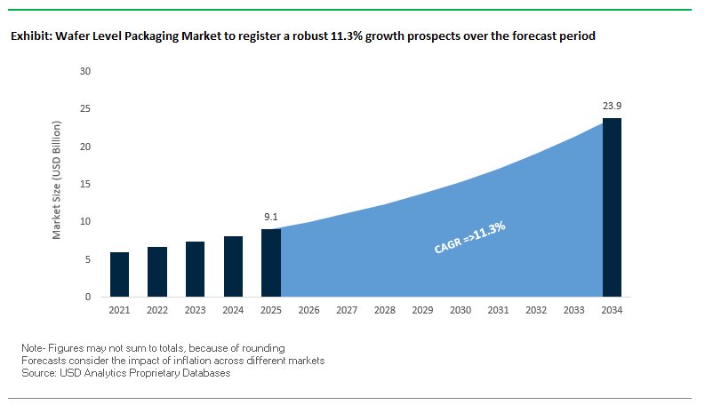
The global wafer level packaging (WLP) market is projected to grow from $9.1 billion in 2025 to $23.9 billion by 2034, at a robust CAGR of 11.3%. WLP technology is central to modern semiconductor manufacturing, enabling smaller, thinner, and more efficient ICs. This growth is driven by increasing demand in consumer electronics, automotive, telecommunications, and AI/high-performance computing applications, where miniaturization, power efficiency, and performance are critical.
Key Insights for industry professionals and buyers:
Circuit miniaturization is fueling the adoption of WLP, particularly for smartphones, wearables, and IoT devices.
Fan-out (FOWLP) and fan-in technologies are gaining traction, offering high I/O counts and improved thermal performance for HPC and AI applications.
System-in-Package (SiP) integration is essential to meet performance demands as Moore’s Law slows, enabling multiple chip functionalities in a single module.
Advanced materials like copper pillars and Through-Silicon Via (TSV) enhance electrical performance, reliability, and power efficiency for next-generation devices.
Strategic focus on 5G, AI, and autonomous vehicle applications is accelerating innovation and driving market expansion.
Market Analysis: Strategic Investments and Technology Innovations Are Accelerating Wafer Level Packaging Growth
The WLP industry is highly dynamic, driven by technological advancements, government initiatives, and strategic capital investments. In August 2025, ASE Technology Holding Co., Ltd. hosted its annual Sustainability Exploration Camp, underscoring its commitment to corporate social responsibility and environmental awareness. In the same month, JCET reported record-high revenue by accelerating investments in advanced packaging technologies, reflecting its global market ambitions.
In July 2025, India’s Netrasemi startup received ₹107 crore in venture capital for smart vision, CCTV, and IoT chip development, highlighting government-backed semiconductor initiatives. Meanwhile, ASE launched its FOCoS-Bridge with TSV technology, reducing power loss by threefold for AI and HPC applications. In May 2025, India’s Union Cabinet approved a HCL-Foxconn joint semiconductor unit with 20,000 wafer-per-month capacity for display driver chips, signaling strategic capacity expansion.
Earlier moves include Amkor Technology establishing a new factory in Bac Ninh, Vietnam (November 2024), strengthening geographic diversification and advanced packaging capacity. Collaborations like Newwen and Parrdekopper’s reusable transport packaging solution (October 2024) emphasize operational efficiency and sustainable logistics in semiconductor manufacturing.
Trends and Opportunities Transforming the Wafer Level Packaging Market
Accelerated Adoption of Fan-Out Wafer Level Packaging (FOWLP) for Heterogeneous Integration
The wafer level packaging (WLP) market is experiencing rapid growth with the adoption of fan-out wafer level packaging (FOWLP) as a foundation for heterogeneous integration. Unlike traditional monolithic chip design, FOWLP enables the integration of multiple chip types—such as CPU, GPU, memory, and I/O—into a single package. This packaging format supports higher interconnection density, reduced interconnect delay, and improved bandwidth, which are vital for advanced computing systems in data centers, AI training, and edge devices.
Commercial adoption is already well established. TSMC’s Integrated Fan-Out (InFO) technology is in high-volume production for mobile processors, offering up to 20% thinner package profiles and 10% better power dissipation compared to earlier solutions. This directly aligns with the industry’s demand for thinner, lighter, and more power-efficient devices, particularly in mobile and consumer electronics.
The rise of chiplet-based architectures is another driver. Industry leaders like AMD and Intel are leveraging chiplets, combining smaller, specialized dies within a single package. This improves yield and reduces cost while allowing integration of heterogeneous components from different process nodes. FOWLP is central to enabling this architectural shift, cementing its role in next-generation semiconductor packaging.
Proliferation of WLP in Automotive-Grade Sensor and Power Applications
The automotive sector is a fast-growing adopter of wafer-level packaging, particularly for ADAS (Advanced Driver-Assistance Systems) and autonomous driving platforms. Vehicles require a dense network of compact, reliable sensors, and WLP provides the necessary miniaturization and reliability. STMicroelectronics, for example, offers automotive-grade inertial sensors packaged in compact system-in-package (SiP) modules, combining accelerometers and gyroscopes for space-constrained vehicle environments.
Beyond sensors, WLP is advancing power electronics packaging for electric vehicles. Infineon Technologies and other key players are leveraging WLP’s improved thermal management and reliability to handle high power densities under harsh automotive conditions. By distributing heat more effectively and ensuring resilience against vibration and temperature extremes, WLP supports the performance and longevity of EV power management systems and automotive-grade semiconductors.
Development of Advanced Materials for Thermal Management and Warpage Control
As semiconductor devices grow more powerful, thermal management and mechanical reliability present critical challenges for wafer-level packaging. Research highlights that integrating graphene layers into FOWLP can reduce average package temperature by 1.6%, improving performance and reliability. Such innovations underscore the role of advanced thermal interface materials in addressing heat dissipation bottlenecks.
Another opportunity lies in addressing wafer warpage, which arises from mismatched Coefficients of Thermal Expansion (CTE) in packaging layers. Warpage can compromise yield and reliability in high-volume manufacturing. Novel low-CTE molding compounds with high glass transition temperatures are being developed to mitigate this issue, ensuring that FOWLP achieves both structural integrity and thermomechanical reliability in demanding applications such as HPC, automotive, and 5G.
Integration of Embedded Passive Components and Antennas at the Wafer Level
Miniaturization demands in IoT, wearables, and smartphones are creating opportunities for embedding passive components such as resistors and capacitors directly at the wafer level. Since these passive components can account for up to 95% of a PCB’s component count, embedding them into the package frees significant board space, reduces design complexity, and supports the continued scaling of compact consumer and industrial devices.
At the same time, the rise of 5G and mmWave technologies is driving the integration of antenna-in-package (AiP) solutions. By embedding antennas within wafer-level packages, the distance between antennas and transceivers is reduced, resulting in improved signal integrity, reduced latency, and higher performance for mmWave communications. For instance, Qualcomm’s Snapdragon SiP platform integrates RF front-end modules and antennas in a single compact package, enabling highly efficient 5G-enabled devices.
Competitive Landscape: Leading OSAT and Semiconductor Players Are Driving Advanced Wafer Level Packaging Solutions
The WLP market is dominated by global leaders leveraging materials science, process innovation, and advanced manufacturing capabilities to deliver high-performance and energy-efficient solutions for electronics, AI, and HPC applications.
ASE Technology Holding Co., Ltd.: Leading Advanced Packaging with FOCoS-Bridge and TSV Innovation
ASE Technology is a global OSAT leader offering 2.5D/3D, fan-out, and SiP solutions critical for AI and HPC. In May 2025, ASE introduced FOCoS-Bridge with TSV technology, significantly reducing power loss. The company’s 2024 US$1.9 billion capital expenditure demonstrates a powerful focus on advanced packaging. ASE’s extensive manufacturing network, R&D investments, and turnkey solutions strengthen its leadership in semiconductor assembly and test.
Amkor Technology provides fan-in and fan-out WLP solutions across multiple industries. In November 2024, the company opened a new facility in Bac Ninh, Vietnam, enhancing its capacity and geographic reach. Amkor’s development of Through Silicon Via (TSV), Through Mold Via (TMV®), and SiP solutions, combined with a portfolio of over 3,000 package formats, underscores its expertise and market breadth.
JCET offers integrated IC services including wafer bumping, assembly, and testing, supporting both fan-in and fan-out WLP technologies. In August 2025, JCET accelerated investment in advanced packaging, achieving record revenue and introducing Co-Packaged Optics (CPO) solutions, improving bandwidth and interconnect efficiency. JCET’s vertical integration and material expertise position it as a leader in the global OSAT market.
Intel Corporation: Pioneering Semiconductor Integration with WLP for High-Performance Computing
Intel develops microprocessors, chipsets, and ICs with advanced WLP solutions for HPC and AI. Its ongoing investment in new materials and packaging technologies supports the next generation of electronics. Intel’s vertically integrated manufacturing and global reach reinforce its dominant brand presence and technology leadership.
Texas Instruments, Inc.: Driving Energy-Efficient Analog and Embedded Processing with WLP Innovations
Texas Instruments focuses on analog and embedded processing semiconductors, leveraging WLP for compact, power-efficient devices. Recent developments include Power Management ICs (PMICs) to improve device energy efficiency. TI’s sustainable materials usage, manufacturing expertise, and global operations strengthen its position in the wafer level packaging sector.
Fan-Out WLP Leads Market Share by Packaging Type in the Wafer-Level Packaging Industry
Fan-Out Wafer-Level Packaging (FO-WLP) accounts for the largest share at nearly 35%, reflecting its critical role in enabling higher I/O density, superior electrical performance, and improved thermal management compared to Fan-In WLP. By reconstituting the wafer and extending interconnects beyond the die area, FO-WLP overcomes the scaling limitations of traditional chip-scale packaging, making it the technology of choice for advanced processors, RF components, and AI accelerators in smartphones and next-generation computing devices. Its dominance is reinforced by the continued miniaturization trend in consumer electronics and the shift toward heterogeneous integration for 5G and high-performance computing applications. As device manufacturers demand thinner, lighter, and more power-efficient chips, FO-WLP remains the benchmark for balancing performance, cost, and scalability.
Consumer Electronics Drive the Largest Market Share by End-Use in the Wafer-Level Packaging Industry
Consumer electronics command about 50% of the wafer-level packaging market, driven by insatiable demand for compact, high-performance devices such as smartphones, wearables, laptops, and tablets. These products rely heavily on both FO-WLP and FI-WLP technologies to deliver miniaturization without compromising power efficiency or speed. As OEMs push for advanced features like higher processing power, 5G/6G connectivity, and enhanced graphics in increasingly smaller form factors, wafer-level packaging has become indispensable. This segment’s dominance is further reinforced by its scale—billions of consumer devices manufactured annually—and its role as the testing ground for next-generation semiconductor packaging innovations before they expand into automotive, IT infrastructure, and healthcare applications.
United States: CHIPS Act, Intel Expansion, and EV-Driven Demand
The United States wafer level packaging (WLP) market is experiencing strong momentum due to the CHIPS and Science Act, which is fostering domestic semiconductor innovation. In April 2024, the U.S. Department of Commerce announced a $5 billion grant program specifically for advanced packaging technologies, including wafer-level packaging, to strengthen local manufacturing resilience. Leading companies like Intel are expanding WLP operations, focusing on next-generation processors and memory chips designed for high-performance computing (HPC), artificial intelligence (AI), and advanced driver-assistance systems (ADAS).
The U.S. market is increasingly emphasizing heterogeneous integration, combining multiple chip types into one package for better performance and power efficiency. Academic institutions such as the Georgia Institute of Technology are advancing disruptive solutions like roll-to-roll WLP and microfluidic cooling systems. Additionally, the surge in electric vehicle (EV) adoption is boosting demand for reliable, compact, and thermally efficient semiconductor components, positioning the U.S. as a leader in next-gen WLP innovation.
European Union: Chips Act Investments and Circular Economy Compliance
The European Union wafer level packaging market is shaped by the European Chips Act, which mobilizes massive investments to strengthen Europe’s role across the semiconductor supply chain. Funding from Horizon Europe is being directed toward research on sustainable semiconductor packaging, including bio-based and compostable materials that could integrate with advanced packaging films.
Regulatory pressures from the Packaging and Packaging Waste Regulation (PPWR), effective February 2025, are pushing WLP manufacturers to adopt recyclable and reusable materials, influencing equipment investments. European companies are carving niches in industrial automation, high-reliability automotive electronics, and medical devices, sectors that demand compact and robust WLP solutions. This dual focus on technological strength and environmental compliance gives Europe a competitive edge in specialized applications.
China: 14th Five-Year Plan, Fan-Out, and 3D Stacking Growth
The China wafer level packaging market is rapidly advancing under the government’s 14th Five-Year Plan, which emphasizes building a self-reliant semiconductor ecosystem. The plan promotes digital and intelligent manufacturing, fostering breakthroughs in advanced packaging technologies. Domestic firms are investing heavily in fan-out wafer-level packaging (FOWLP) and 3D stacking, key solutions for consumer electronics, 5G, and telecom infrastructure.
A growing trend is the development of high-end packaging with enhanced barrier properties and anti-counterfeiting features, reflecting both consumer electronics demand and regulatory oversight. With strong government backing and tax incentives for green technology adoption, China is set to solidify its role as a global hub for advanced WLP solutions.
India: PLI/DLI Schemes and OSAT Ecosystem Development
The India wafer level packaging market is emerging with strong government support through the Production Linked Incentive (PLI) and Design Linked Incentive (DLI) schemes. These initiatives, backed by billions in funding, are accelerating domestic capacity in semiconductor assembly, testing, and packaging. The India Semiconductor Mission (ISM) is steering OSAT (Outsourced Semiconductor Assembly and Test) investments, with projects that incorporate wafer-level packaging and testing facilities.
India is also building its ecosystem with a National Single Window System for streamlined approvals and plug-and-play semiconductor parks to attract global players. Programs like Chips to Startup (C2S) are strengthening the skilled workforce needed to sustain industry growth. Together, these policies are positioning India as a future outsourcing hub for advanced WLP services, especially for global fabless companies.
Japan: BBCube™, High-Speed Bonding, and METI Support
The Japan wafer level packaging market is driven by its long-standing leadership in precision engineering and advanced materials. Researchers at the Institute of Science Tokyo developed BBCube™, a novel 2.5D/3D integration approach that enhances performance and power efficiency, directly impacting high-performance computing applications. Japanese companies are also pioneering high-speed bonding techniques and advanced adhesives for 3D integration, ensuring reliability in automotive and industrial markets.
Government support through the Ministry of Economy, Trade and Industry (METI) is strengthening Japan’s semiconductor revival strategy, with a particular focus on advanced packaging, materials, and equipment. This, combined with Japan’s tradition of R&D excellence, ensures the country remains a global leader in next-generation WLP technologies.
Taiwan: TSMC Leadership and Fan-Out Packaging Dominance
The Taiwan wafer level packaging market is the most established globally, with TSMC leading advancements in fan-out wafer-level packaging (FOWLP). Taiwan’s dominance in consumer electronics and automotive chips ensures a steady demand for WLP solutions that deliver higher I/O density, superior electrical performance, and better thermal management.
Taiwanese firms remain pioneers in scaling 3D IC packaging and heterogeneous integration, solidifying their role as indispensable partners for global fabless semiconductor companies. With a combination of world-class foundries, OSAT expertise, and a strong innovation pipeline, Taiwan continues to anchor the global WLP supply chain.
Wafer Level Packaging Market Report Scope
Wafer Level Packaging Market
Parameter
Details
Market Size (2025)
$9.1 Billion
Market Size (2034)
$23.9 Billion
Market Growth Rate
11.3%
Segments
By Packaging Type (FI-WLP, FO-WLP, WLCSP, 3D TSV WLP, 2.5D TSV WLP, Nano WLP), By Technology (Electrochemical Deposition, Physical Vapor Deposition, Etch, Chemical Vapor Deposition, Chemical Mechanical Planarization, Other Technologies), By End-Use Industry (Consumer Electronics, IT & Telecommunication, Automotive, Healthcare, Aerospace & Defense, Industrial), By Application (Analog & Mixed-Signal Devices, MEMS, RF Devices, PMICs, Sensors, Other Applications)
Study Period
2019- 2024 and 2025-2034
Units
Revenue (USD)
Qualitative Analysis
Porter’s Five Forces, SWOT Profile, Market Share, Scenario Forecasts, Market Ecosystem, Company Ranking, Market Dynamics, Industry Benchmarking
Companies
Advanced Semiconductor Engineering (ASE), Amkor Technology, Taiwan Semiconductor Manufacturing Company (TSMC), Intel Corporation, JCET Group Co., Ltd., Samsung Electronics Co., Ltd., Lam Research Corporation, Applied Materials, Inc., Deca Technologies Inc., Fujitsu Limited, Tokyo Electron Ltd., Unisem (M) Berhad, Powertech Technology Inc., Chipbond Technology Corporation, Siliconware Precision Industries Co., Ltd. (SPIL)
Countries
US, Canada, Mexico, Germany, France, Spain, Italy, UK, Russia, China, India, Japan, South Korea, Australia, South East Asia, Brazil, Argentina, Middle East, Africa
Wafer Level Packaging Market Segmentation
By Packaging Type
FI-WLP
FO-WLP
WLCSP
3D TSV WLP
2.5D TSV WLP
Nano WLP
By Technology
Electrochemical Deposition
Physical Vapor Deposition
Etch
Chemical Vapor Deposition
Chemical Mechanical Planarization
Other Technologies
By End-Use Industry
Consumer Electronics
IT & Telecommunication
Automotive
Healthcare
Aerospace & Defense
Industrial
By Application
Analog & Mixed-Signal Devices
MEMS
RF Devices
PMICs
Sensors
Other Applications
Countries Analyzed
North America (US, Canada, Mexico)
Europe (Germany, UK, France, Spain, Italy, Russia, Rest of Europe)
Asia Pacific (China, India, Japan, South Korea, Australia, South East Asia, Rest of Asia)
South America (Brazil, Argentina, Rest of South America)
Middle East and Africa (Saudi Arabia, UAE, Rest of Middle East, South Africa, Egypt, Rest of Africa)
Top Companies in Wafer Level Packaging Market
Advanced Semiconductor Engineering (ASE)
Amkor Technology
Taiwan Semiconductor Manufacturing Company (TSMC)
Intel Corporation
JCET Group Co., Ltd.
Samsung Electronics Co., Ltd.
Lam Research Corporation
Applied Materials, Inc.
Deca Technologies Inc.
Fujitsu Limited
Tokyo Electron Ltd.
Unisem (M) Berhad
Powertech Technology Inc.
Chipbond Technology Corporation
Siliconware Precision Industries Co., Ltd. (SPIL)
* List Not Exhaustive
Methodology
USDAnalytics employs a rigorous, multi-step research methodology to deliver comprehensive insights into the global wafer level packaging (WLP) market. Our approach combines primary data collection from semiconductor manufacturers, OSAT providers, and industry experts with secondary research, including company reports, regulatory filings, academic studies, and market databases. The study evaluates key growth drivers such as miniaturization trends, fan-out and fan-in packaging adoption, heterogeneous integration, and high-performance computing applications, alongside technological innovations like TSV, advanced materials, embedded passive components, and antenna-in-package (AiP) solutions. Regional dynamics across North America, Europe, China, India, Japan, Taiwan, and emerging markets are analyzed with respect to government initiatives, capacity expansions, and strategic investments. USDAnalytics’ methodology further incorporates segmentation by packaging type, technology, end-use industry, and application, providing actionable intelligence for semiconductor manufacturers, OSATs, and technology investors seeking to capitalize on the evolving WLP landscape, optimize design efficiency, and enhance cost-performance outcomes for next-generation electronic devices.
Deliverables:
Comprehensive Market Research Report (PDF and Excel) with detailed tables, charts, and interactive visualizations.
Country-Specific Forecasts & Analysis.
Segment-Wise Revenue Forecasts (2025–2034).
Competitive Analysis, Benchmarking, and SWOT Profiles.
Recent Developments & Innovation Tracker.
Executive Summary & Analyst Commentary.
Post-Purchase Analyst Support for Client-Specific Questions and Custom Data Requirements.
Table of Contents: Wafer Level Packaging (WLP) Market
1. Executive Summary
1.1. Market Highlights
1.2. Key Findings
1.3. Global Market Snapshot
2. Wafer Level Packaging Market Landscape & Outlook (2025–2034)
2.1. Introduction to Wafer Level Packaging Market
2.2. Market Valuation and Growth Projections (2025–2034)
2.3. Strategic Investments Driving Market Expansion
2.4. Government Initiatives and Policy Support
2.5. Geographic Expansion and Capacity Development
3. Innovations Reshaping the Wafer Level Packaging Market
3.1. Trend: Accelerated Adoption of Fan-Out Wafer Level Packaging (FOWLP) for Heterogeneous Integration
3.2. Trend: Proliferation of WLP in Automotive-Grade Sensor and Power Applications
3.3. Opportunity: Development of Advanced Materials for Thermal Management and Warpage Control
3.4. Opportunity: Integration of Embedded Passive Components and Antennas at the Wafer Level
4. Competitive Landscape and Strategic Initiatives
4.1. Mergers, Acquisitions and Strategic Alliances
4.2. R&D and Material Innovation
4.3. Sustainability and Strategies
4.4. Market Expansion and Regional Focus
5. Market Share and Segmentation Insights: Wafer Level Packaging Market
5.1. By Packaging Type
5.1.1. FI-WLP
5.1.2. FO-WLP
5.1.3. WLCSP
5.1.4. 3D TSV WLP
5.1.5. 2.5D TSV WLP
5.1.6. Nano WLP
5.2. By Technology
5.2.1. Electrochemical Deposition
5.2.2. Physical Vapor Deposition
5.2.3. Etch
5.2.4. Chemical Vapor Deposition
5.2.5. Chemical Mechanical Planarization
5.2.6. Other Technologies
5.3. By End-Use Industry
5.3.1. Consumer Electronics
5.3.2. IT & Telecommunication
5.3.3. Automotive
5.3.4. Healthcare
5.3.5. Aerospace & Defense
5.3.6. Industrial
5.4. By Application
5.4.1. Analog & Mixed-Signal Devices
5.4.2. MEMS
5.4.3. RF Devices
5.4.4. PMICs
5.4.5. Sensors
5.4.6. Other Applications
6. Country Analysis and Outlook of Wafer Level Packaging Market
6.1. United States
6.2. Canada
6.3. Mexico
6.4. Germany
6.5. France
6.6. Spain
6.7. Italy
6.8. UK
6.9. Russia
6.10. China
6.11. India
6.12. Japan
6.13. South Korea
6.14. Australia
6.15. South East Asia
6.16. Brazil
6.17. Argentina
6.18. Middle East
6.19. Africa
7. Wafer Level Packaging Market Size Outlook by Region (2025–2034)
7.1. North America WLP Market Size Outlook to 2034
7.1.1. By Packaging Type
7.1.2. By Technology
7.1.3. By End-Use Industry
7.1.4. By Application
7.2. Europe WLP Market Size Outlook to 2034
7.2.1. By Packaging Type
7.2.2. By Technology
7.2.3. By End-Use Industry
7.2.4. By Application
7.3. Asia Pacific WLP Market Size Outlook to 2034
7.3.1. By Packaging Type
7.3.2. By Technology
7.3.3. By End-Use Industry
7.3.4. By Application
7.4. South America WLP Market Size Outlook to 2034
7.4.1. By Packaging Type
7.4.2. By Technology
7.4.3. By End-Use Industry
7.4.4. By Application
7.5. Middle East and Africa WLP Market Size Outlook to 2034
7.5.1. By Packaging Type
7.5.2. By Technology
7.5.3. By End-Use Industry
7.5.4. By Application
8. Company Profiles: Leading Players in the Wafer Level Packaging Market
8.1. Advanced Semiconductor Engineering (ASE)
8.2. Amkor Technology
8.3. Taiwan Semiconductor Manufacturing Company (TSMC)
8.4. Intel Corporation
8.5. JCET Group Co., Ltd.
8.6. Samsung Electronics Co., Ltd.
8.7. Lam Research Corporation
8.8. Applied Materials, Inc.
8.9. Deca Technologies Inc.
8.10. Fujitsu Limited
8.11. Tokyo Electron Ltd.
8.12. Unisem (M) Berhad
8.13. Powertech Technology Inc.
8.14. Chipbond Technology Corporation
8.15. Siliconware Precision Industries Co., Ltd. (SPIL)
9. Methodology
9.1. Research Scope
9.2. Market Research Approach
9.3. Market Sizing and Forecasting Model
9.4. Research Coverage
9.5. Data Horizon
9.6. Deliverables
10. Appendix
10.1. Acronyms and Abbreviations
10.2. List of Tables
10.3. List of Figures
Wafer Level Packaging Market Segmentation
By Packaging Type
FI-WLP
FO-WLP
WLCSP
3D TSV WLP
2.5D TSV WLP
Nano WLP
By Technology
Electrochemical Deposition
Physical Vapor Deposition
Etch
Chemical Vapor Deposition
Chemical Mechanical Planarization
Other Technologies
By End-Use Industry
Consumer Electronics
IT & Telecommunication
Automotive
Healthcare
Aerospace & Defense
Industrial
By Application
Analog & Mixed-Signal Devices
MEMS
RF Devices
PMICs
Sensors
Other Applications
Countries Analyzed
North America (US, Canada, Mexico)
Europe (Germany, UK, France, Spain, Italy, Russia, Rest of Europe)
Asia Pacific (China, India, Japan, South Korea, Australia, South East Asia, Rest of Asia)
South America (Brazil, Argentina, Rest of South America)
Middle East and Africa (Saudi Arabia, UAE, Rest of Middle East, South Africa, Egypt, Rest of Africa)
The global wafer level packaging market is expected to grow from USD 9.1 billion in 2025 to USD 23.9 billion by 2034, registering a CAGR of 11.3%. Growth is driven by increasing demand in consumer electronics, automotive, AI/high-performance computing, and 5G applications, where miniaturization, efficiency, and heterogeneous integration are key.
Fan-Out Wafer-Level Packaging (FO-WLP) leads the market with nearly 35% share. Its ability to provide higher I/O density, improved electrical performance, and superior thermal management makes it ideal for smartphones, AI accelerators, and next-generation processors. FO-WLP also supports thinner, lighter, and more power-efficient devices.
WLP is widely adopted in automotive sensors, ADAS modules, and EV power electronics, providing compact, reliable packaging with excellent thermal management and vibration resilience. In HPC and AI devices, WLP improves interconnect density, reduces latency, and supports heterogeneous integration, enhancing performance and energy efficiency.
North America and Europe benefit from CHIPS Act and Horizon Europe investments, supporting domestic manufacturing and sustainable packaging. China is expanding fan-out and 3D stacking capabilities under the 14th Five-Year Plan, while India leverages PLI/DLI schemes to build an OSAT ecosystem. Taiwan and Japan continue to lead in precision WLP technologies, driven by consumer electronics and high-performance computing demand.