Patterning Materials Market Overview 2025–2034: $8.7 Billion Market Size in 2025 Expanding at 5.7% CAGR Driven by High-NA EUV and 2nm Node Transition
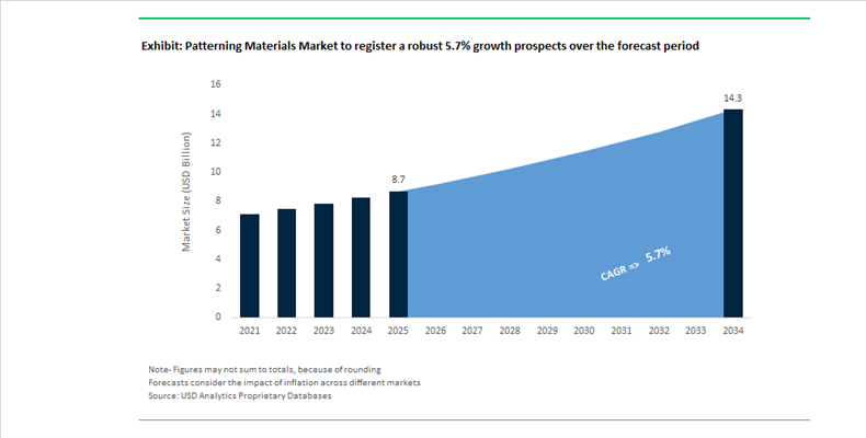
The Patterning Materials Market is valued at $8.7 billion in 2025 and is projected to reach $14.3 billion by 2034, advancing at a CAGR of 5.7%. Growth is being propelled by accelerating semiconductor node shrinkage, High-NA EUV lithography adoption, advanced packaging integration, and AI-driven materials discovery. Patterning materials including EUV photoresists, ArF immersion resists, metal-oxide resists, spin-on hardmasks, and nanoimprint lithography materials form the backbone of sub-5nm and emerging 2nm logic fabrication. Demand expansion is closely aligned with generative AI processor manufacturing, high-bandwidth memory scaling, and regional fab investments in South Korea, Japan, Europe, and the United States.
Throughout 2024 and 2025, the industry validated the performance of metal-oxide resists (MOR) for 2nm logic nodes. JSR and its subsidiary Inpria confirmed successful process integration of tin-based inorganic resists, which provide superior etch resistance and resolution compared to traditional chemically amplified resists. The transition toward MOR chemistry reflects the need for improved line-edge roughness control and pattern fidelity at feature sizes approaching 8nm resolution. By late 2025, ASML’s 0.55 NA High-NA EUV systems transitioned from pilot phases to high-volume manufacturing, creating structural demand for next-generation EUV resists compatible with increased numerical aperture and tighter process windows. This shift is fundamentally redefining material design criteria across the lithography ecosystem.
Strategic consolidation and capacity localization intensified during 2025. In February 2025, Tokyo Ohka Kogyo completed the full acquisition of micro resist technology GmbH in Germany, expanding its nanoimprint lithography and photonic resist portfolio within the European high-tech corridor. In August 2025, TOK announced construction of a new advanced photoresist manufacturing plant in Pyeongtaek, South Korea, ensuring localized supply for Samsung and SK Hynix fabs supporting AI-driven semiconductor expansion. In September 2025, TOK joined the JOINT3 consortium to optimize back-end patterning materials for redistribution layer and through-silicon via processes in 3D-stacked chip architectures. These developments highlight the increasing integration of front-end and advanced packaging material strategies.
Capital expenditure and R&D investments reached record levels. In November 2025, FUJIFILM completed a ¥13 billion expansion at its Shizuoka facility, equipped with AI-enabled quality control systems to accelerate EUV and ArF resist development. This facility forms part of a broader ¥100 billion semiconductor materials investment plan through 2026. Earlier in 2025, Fujifilm introduced PFAS-free ArF immersion resists developed with imec, addressing tightening regulatory restrictions on fluorinated surfactants in semiconductor fabrication. AI integration into material discovery also gained momentum. In December 2024, MaterialsZone launched an AI-guided formulation simulation platform increasingly adopted by specialty chemical firms to reduce experimental cycles in resist optimization. In November 2025, JSR and IBM initiated a joint generative AI research program focused on accelerating molecular discovery for sub-2nm photoresist chemistry, significantly shortening development timelines for future logic nodes.
Market outlook for 2026 reflects continued electronics recovery and structural AI demand. In January 2026, Shin-Etsu Chemical reported sustained capital spending to support ArF and EUV resist expansion amid new fab startups. In February 2026, DuPont projected net sales of up to $7.135 billion, citing semiconductor-driven organic growth in its patterning materials portfolio. The Patterning Materials Market is therefore positioned at the intersection of High-NA EUV adoption, inorganic resist innovation, AI-assisted molecular design, localized supply chain expansion, and advanced packaging integration supporting next-generation semiconductor manufacturing.
Patterning Materials Market Trends and Opportunities: Sub-2nm Transition, EUV Disruption, and Next-Gen Lithography Materials
High-NA EUV Lithography Driving Fundamental Shift from CARs to Metal-Oxide Resists
The Patterning Materials market is undergoing a paradigm shift as semiconductor manufacturing transitions toward sub-2nm nodes, where conventional Chemically Amplified Resists (CARs) are reaching fundamental resolution and stochastic limits. The adoption of High Numerical Aperture (High-NA) EUV lithography (0.55 NA) is redefining material requirements, accelerating the shift toward metal-containing resists (MORs) and hybrid resist chemistries optimized for extreme pattern fidelity.
The transition reached a critical milestone in late 2025 and early 2026, with High-NA EUV systems entering high-volume manufacturing (HVM), enabling a 2.9× increase in transistor density and resolving features down to 8nm critical dimensions. This has intensified R&D investment in sensitivity-resolution-roughness (SRR) optimization, a key performance metric for advanced patterning materials. At the 2026 SPIE Advanced Lithography + Patterning Conference, innovations such as DuPont’s EON™ EUV photoresist platform demonstrated targeted solutions for stochastic defectivity, a major bottleneck at advanced nodes.
From an economic standpoint, the scale of this transition is substantial. Deloitte’s 2026 Semiconductor Outlook estimates $30 billion in global spending on patterning technologies, driven by the rapid migration from 3nm nodes (2025) to 2nm and 1.8nm nodes (2026). This is positioning advanced EUV-compatible materials as a high-value segment within semiconductor materials markets, with strong demand for next-generation resist platforms capable of enabling atomic-scale precision.
Supply Chain Regionalization and “China Plus One” Strategy Reshaping Semiconductor Material Sourcing
Geopolitical dynamics and the strategic imperative of technology sovereignty are driving structural changes in the Patterning Materials supply chain. The traditional dependence on China for specialty chemicals and intermediates is being replaced by a multi-node, geographically diversified sourcing model, commonly referred to as the “China Plus One” strategy.
By 2026, over 70% of semiconductor material companies have adopted dual-sourcing strategies, with increasing investments in Vietnam, Malaysia, and Thailand for midstream chemical processing. This shift is aimed at mitigating single-country concentration risks while ensuring supply continuity for critical patterning materials such as photoresists, developers, and specialty gases.
Policy interventions are further accelerating localization. Under the U.S. CHIPS and Science Act, reports indicate that nearly 60% of front-end wafer chemicals remain import-dependent, prompting approximately $9 billion in new capital investment to establish domestic manufacturing capabilities. Concurrently, supply chain volatility in early 2026, triggered by interventions in major semiconductor firms, has redefined inventory strategies. Companies are increasingly adopting “inventory-as-a-strategic-buffer” models, extending stockpiles by 6 to 8 weeks to safeguard production continuity.
This evolving supply chain landscape is elevating resilience, localization, and supply assurance as critical competitive parameters in the Patterning Materials market.
Dry Resist Technology Emerging as a Critical Enabler for High-NA EUV and Advanced DRAM Scaling
Dry resist technology represents a transformative opportunity in the Patterning Materials market, addressing key limitations of traditional spin-on (wet) photoresist systems, including pattern collapse, excessive chemical consumption, and line-edge roughness (LER). Applied via vapor deposition techniques, dry resists offer a scalable pathway for sub-2nm lithography and next-generation memory fabrication.
Commercial adoption is already underway. In January 2025, Lam Research announced that its Aether® dry photoresist technology had been selected as the production tool of record for advanced DRAM manufacturing, marking a significant transition from pilot-stage validation to high-volume manufacturing deployment. This validates dry resist as a production-ready solution for advanced semiconductor nodes.
From a sustainability and efficiency perspective, dry resist processes consume 5 to 10 times less chemical volume compared to wet processes, aligning with semiconductor fabs’ goals for chemical waste reduction and environmental compliance. Additionally, the elimination of liquid developers mitigates surface tension effects, significantly improving pattern fidelity and reducing LER in high-aspect-ratio structures.
Crucially, dry resist technology enhances EUV scanner productivity by enabling patterning at lower exposure doses, directly improving throughput. This is particularly relevant for AI-driven computing and next-generation DRAM scaling, where demand for higher memory density in smaller footprints continues to surge. As a result, dry resist is emerging as a core enabling technology for high-performance semiconductor manufacturing ecosystems.
Directed Self-Assembly (DSA) Unlocking Cost-Efficient Pattern Multiplication and Resolution Enhancement
Directed Self-Assembly (DSA) of block copolymers (BCPs) is gaining traction as a complementary patterning technique that enhances the capabilities of EUV lithography while reducing overall process costs. As EUV exposure costs escalate, DSA provides a bottom-up approach to pattern refinement and pitch multiplication, enabling manufacturers to achieve sub-2nm feature scaling with improved uniformity.
Recent research highlights the effectiveness of the “EUV + DSA hybrid strategy”, where DSA compensates for imperfections in initial lithographic exposures. Studies indicate that DSA can reduce EUV dose requirements by 30% to 50%, while improving local critical dimension uniformity (LCDU) and minimizing stochastic defects. This significantly enhances yield and process stability at advanced nodes.
Technical advancements in high-χ (chi) block copolymers are enabling perpendicular domain alignment at dimensions compatible with 1.5nm nodes, pushing the boundaries of nanoscale fabrication. Leading semiconductor firms have successfully integrated DSA into manufacturing workflows, demonstrating sub-10nm resolution enhancement and improved pattern fidelity.
From a cost perspective, DSA offers a compelling alternative to traditional multi-patterning techniques, which require multiple EUV exposures per layer. By enabling self-aligned pitch multiplication, DSA can reduce cost-per-wafer by double-digit percentages, making it highly attractive for both advanced logic and DRAM fabrication. This positions DSA as a high-impact, cost-optimization lever within the Patterning Materials market, particularly in the era of escalating lithography complexity.
Patterning Materials Market Share and Segmentation Insights
Photoresists Lead Semiconductor Patterning Materials Demand in Advanced EUV Lithography Processes
Photoresists accounted for 48.60% of the Patterning Materials Market by material type in 2025, reflecting their central role in semiconductor photolithography processes used to transfer circuit patterns onto silicon wafers. These light sensitive polymer materials are essential in advanced semiconductor manufacturing where increasingly complex integrated circuit designs require highly precise pattern transfer. As semiconductor nodes continue scaling toward 3nm, 2nm, and sub-2nm technologies, demand for advanced photoresist materials has increased significantly. In 2025, the industry focus on EUV photoresist innovation for 13.5 nm lithography exposure is accelerating development of new polymer chemistries, photoacid generators, and underlayer systems optimized for extreme ultraviolet lithography used in leading edge semiconductor fabrication.
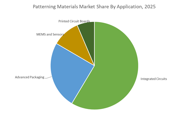
Integrated Circuits Segment Drives Patterning Material Consumption in Advanced Chip Manufacturing
Integrated circuits represented 58.60% of the Patterning Materials Market by application in 2025, reflecting the intensive use of photolithography materials in logic, memory, and processor manufacturing. Semiconductor fabrication requires dozens of patterning steps per wafer, often ranging from 50 to 100 lithography layers, each consuming photoresists, anti reflective coatings, developers, and hardmask materials. As transistor densities increase and chip architectures become more complex, the consumption of patterning materials continues to expand. In 2025, the adoption of multi patterning lithography techniques such as LELE, SADP, and SAQP is significantly increasing material usage per wafer layer, supporting demand growth even as wafer fabrication volumes remain relatively stable.
Patterning Materials Market Competitive Landscape
The Patterning Materials Market is defined by High-NA EUV lithography, PFAS-free photoresists, and Nanoimprint Lithography (NIL) innovation. Leading players are investing in advanced resist chemistries, AI-driven materials discovery, and localized semiconductor supply chains to support sub-10nm nodes and AI-driven chip manufacturing.
TOK accelerates multi-trigger resist development and expands EUV photoresist capacity in Asia
Tokyo Ohka Kogyo Co., Ltd. (TOK) is strengthening its leadership in patterning materials through next-generation resist innovation and regional capacity expansion. Its strategic partnership with Irresistible Materials is advancing the MTR™ platform, enabling ultra-fine patterning for High-NA EUV lithography at scales significantly smaller than traditional polymer resists. The construction of its Pyeongtaek facility enhances localized supply of high-purity photoresists for major semiconductor fabs in South Korea. TOK is also focusing on PFAS/PFOS-free and metal-free formulations, aligning with sustainability mandates. The acquisition of micro resist technology GmbH expands its portfolio into MEMS and photonic applications. This combination of advanced chemistry, capacity expansion, and sustainability focus reinforces TOK’s market dominance.
Shin-Etsu scales vertically integrated EUV materials with strong financial and R&D backbone
Shin-Etsu Chemical Co., Ltd. maintains a strong competitive position through its vertically integrated electronics materials portfolio, spanning silicon wafers, photomask blanks, and photoresists. With projected FY2026 sales of ¥2.4 trillion and operating income of ¥635 billion, the company demonstrates robust financial strength. Its ¥500 billion share buyback program reflects high liquidity and strategic confidence. Shin-Etsu is focusing on expanding EUV photoresist production and high-performance silicones to support advanced semiconductor nodes. Its recognition as a Top 100 Global Innovator for 14 consecutive years highlights its ability to rapidly commercialize R&D breakthroughs. This integration of scale, innovation, and financial stability strengthens its leadership in advanced patterning materials.
Qnity expands advanced node materials and CMP infrastructure for AI semiconductor manufacturing
Qnity (formerly DuPont Electronics) is emerging as a focused leader in advanced patterning materials following its spin-off, concentrating on high-performance computing and advanced packaging. The opening of its Delaware manufacturing facility enhances production of CMP components critical for wafer planarization in AI chip fabrication. Its acquisition of a semiconductor facility in Taiwan strengthens proximity to major foundries and supports advanced node material development. With $4.75 billion in 2025 sales and strong growth in its Semiconductor Technologies segment, Qnity is capitalizing on demand for next-generation materials. Its streamlined capital allocation enables continued investment in advanced packaging and connectivity applications. This targeted strategy positions Qnity as a key player in the Angstrom-era semiconductor ecosystem.
Fujifilm advances PFAS-free EUV resists and NIL technologies for next-generation chip fabrication
Fujifilm Corporation is accelerating its growth in patterning materials through innovation in EUV resists and Nanoimprint Lithography solutions. The company is developing negative-tone EUV resists and PFAS-free ArF immersion resists to address both miniaturization and environmental challenges. Its leadership in NIL materials, including UV-curable resists, offers cost-effective alternatives to traditional EUV processes. Fujifilm aims to double semiconductor materials revenue to ¥500 billion by 2030, driven by demand from AI GPUs and HBM memory. Strategic investment in the Rapidus 2nm foundry project secures its role in next-generation chip manufacturing. This combination of innovation, sustainability, and strategic partnerships strengthens Fujifilm’s competitive position.
JSR integrates AI-driven materials discovery and MOR technology for EUV patterning efficiency
JSR Corporation is advancing its position in the patterning materials market through AI-enabled R&D and next-generation resist technologies. Its collaboration with Lam Research integrates Metal Oxide Resist (MOR) with advanced processing techniques to improve EUV patterning efficiency. Partnership with IBM leverages AI and quantum simulations to accelerate discovery of high-performance polymers and patterning materials. The company’s portfolio optimization strategy, including divestment of non-core businesses, allows full focus on lithography materials and life sciences. JSR’s sustainability initiatives, including closed-loop water systems, have earned high environmental performance ratings. This integration of digital innovation, advanced materials, and sustainability positions JSR as a technology leader.
United States – High-NA EUV Commercialization Reshaping Materials Demand
The United States has moved decisively into first-mover territory in next-generation patterning materials following the operational deployment of High-NA EUV lithography. In February 2025, Intel became the first chipmaker to bring ASML’s EXE:5000 High-NA EUV systems into production in Oregon. Initial operational data confirmed throughput of approximately 30,000 wafers in a single quarter, alongside reliability levels roughly double those of prior EUV platforms. This shift has direct implications for the patterning materials ecosystem, as High-NA adoption fundamentally alters photoresist performance requirements, defect tolerance thresholds, and process window optimization.
Material consumption patterns are changing in parallel. Intel’s 2025 technical briefings confirmed that High-NA EUV eliminated the need for triple-patterning in critical layers, collapsing three exposures and nearly 40 downstream process steps into a single exposure. This has materially reduced demand for specialty developers, strippers, and hardmask refresh chemistries, while increasing the strategic value of ultra-high-resolution resists with superior line-edge roughness control. Policy support under the CHIPS and Science Act has reinforced this transition. The U.S. Department of Commerce is explicitly funding the domestic materials ecosystem, prompting Fujifilm and DuPont to expand advanced photoresist manufacturing in Texas and Delaware. Concurrently, the National Semiconductor Technology Center, operationalized in 2025, has prioritized materials informatics, applying AI-driven discovery to compress sub-2nm patterning chemistry development cycles from years to months.
South Korea – Capital Intensity and Localized EUV Materials Resilience
South Korea remains one of the most capital-intensive markets for advanced patterning materials, driven by aggressive logic and memory roadmaps. In October 2025, Samsung Electronics announced a ₩47.4 trillion capital expenditure plan, with approximately ₩40.9 trillion allocated to its Device Solutions division. A substantial portion of this investment is directed toward upgrading fabrication lines for High-Bandwidth Memory and advanced logic nodes, both of which require highly specialized photoresists, hardmasks, and sacrificial materials.
Supply chain resilience has emerged as a defining theme. Following prior disruptions, Samsung and SK Hynix intensified collaboration with domestic suppliers such as Dongjin Semichem to commercialize localized EUV photoresists. This localization strategy reduces dependence on imported Japanese materials for critical layers. At the same time, Samsung is progressing toward volume production of its 2nm process by late 2025, built on second-generation nanosheet transistor architectures. These designs demand high-selectivity etch chemistries and thermally stable hardmasks. Beyond semiconductors, Samsung Display received ₩3.3 trillion in 2025 funding to advance OLED patterning, reinforcing demand for fine metal masks and photo-imageable polyimides that sit adjacent to core semiconductor patterning materials.
Taiwan – Logic Node Leadership Driving BEOL and Packaging Materials Innovation
Taiwan continues to define the global performance frontier for patterning materials through its leadership in advanced logic manufacturing. At the 2025 technology symposium, TSMC accelerated its A16 roadmap, integrating nanosheet transistors with Super Power Rail architectures. This evolution requires a comprehensive redesign of backend-of-line patterning materials, particularly for metal line definition, dielectric etch selectivity, and via integrity at extreme scaling.
Capacity expansion is amplifying materials demand. TSMC plans to construct nine new facilities during 2025, including eight wafer fabs, with Fab 20 in Hsinchu and Fab 22 in Kaohsiung serving as primary 2nm production sites. Volume production of the N2 node is scheduled for the fourth quarter of 2025, leveraging new metal-oxide resists that deliver approximately 1.15x higher chip density compared with N3E. In parallel, the expansion of CoWoS advanced packaging capacity across 2025 and 2026 is driving strong demand for thick-layer photoresists, polyimide dielectrics, and redistribution layer materials used in 3D integrated circuit stacking. As a result, Taiwan’s influence on global patterning materials increasingly extends beyond front-end lithography into advanced packaging chemistries.
Japan – Materials Science Leadership and EUV Chemistry Innovation
Japan remains the global innovation anchor for patterning materials, particularly in photoresists and photomask substrates. In November 2025, JSR Corporation and IBM launched a joint program applying generative AI to chemical materials discovery. The initiative uses foundational models to simulate molecular structures for next-generation EUV resists, significantly accelerating formulation optimization for sub-2nm nodes.
Commercial progress in metal oxide resists has further strengthened Japan’s position. At SEMICON Japan 2025, JSR demonstrated MOR platforms with higher EUV absorption coefficients and improved etch resistance versus conventional organic polymers. These attributes are increasingly critical as feature sizes approach atomic dimensions. Broader industry investment supports this momentum. Shin-Etsu Chemical reported a 6.1% increase in net sales in 2025, with capital expenditures focused on synthetic quartz for photomasks and photoresist intermediates. Meanwhile, Japan continues to dominate mature lithography segments. Companies such as Tokyo Ohka Kogyo are retrofitting i-Line and g-Line resist facilities to serve renewed demand from automotive and power semiconductor manufacturing.
China – Materials-First Strategy Under EUV Constraints
China’s patterning materials strategy in 2025 has been shaped by technology access constraints and a deliberate pivot toward self-reliance. In December 2025, reports indicated the completion of a domestic EUV lithography prototype in Shenzhen. While commercial deployment is not expected before 2028, the effort has catalyzed a nationwide “materials-first” policy emphasizing photoresists, monomers, and ultra-high-purity process chemicals.
Progress at mature nodes has been substantial. By 2025, China achieved more than 70% self-sufficiency in i-Line and KrF photoresists, with firms such as Nata Opto-electronic and Crystal Clear Electronic Material scaling ArF resist production. State-backed capital has reinforced this trajectory. Phase III of the national semiconductor investment vehicle, commonly known as the Big Fund, has concentrated 2025 funding on bottleneck segments including photoresist monomers and high-purity CMP slurries. As a result, China’s patterning materials market is increasingly characterized by volume scaling at DUV nodes and long-term capability building for advanced lithography.
Comparative Snapshot – Patterning Materials Industry by Country
Patterning Materials Market County Level Snapshot
|
Country
|
Strategic Focus
|
Key Driver
|
Structural Impact
|
|
United States
|
High-NA EUV commercialization
|
CHIPS Act and AI-driven materials discovery
|
Reduced multi-patterning, premium resist demand
|
|
South Korea
|
Capital-led node advancement
|
Logic and HBM investments
|
Localization of EUV photoresists
|
|
Taiwan
|
Logic and packaging leadership
|
Nanosheet and CoWoS expansion
|
Growth in BEOL and thick-layer materials
|
|
Japan
|
Materials science innovation
|
AI-driven EUV chemistry and MORs
|
Technology leadership in sub-2nm resists
|
|
China
|
Self-reliance under constraints
|
Materials-first industrial policy
|
Rapid scaling in DUV and precursor segments
|
Patterning Materials Market Report Scope
Patterning Materials Market
|
Parameter
|
Details
|
|
Market Size (2025)
|
$8.7 Billion
|
|
Market Size (2034)
|
$14.3 Billion
|
|
Market Growth Rate
|
5.7%
|
|
Segments
|
By Material Type (Photoresists, Anti-Reflective Coatings, Developers, Hardmasks, Primers and Adhesion Promoters, Photoresist Strippers and Edge Bead Removers), By Application (Integrated Circuits, Advanced Packaging, Printed Circuit Boards, MEMS and Sensors)
|
|
Study Period
|
2019- 2025 and 2026-2034
|
|
Units
|
Revenue (USD)
|
|
Qualitative Analysis
|
Porter’s Five Forces, SWOT Profile, Market Share, Scenario Forecasts, Market Ecosystem, Company Ranking, Market Dynamics, Industry Benchmarking
|
|
Companies
|
JSR Corporation, Tokyo Ohka Kogyo, Shin-Etsu Chemical, Fujifilm, DuPont, Merck, Sumitomo Chemical, Resonac Holdings, Dongjin Semichem, Honeywell, Allresist, Kayaku Advanced Materials, Brewer Science, Nata Opto-electronic Material, Dow
|
|
Countries
|
US, Canada, Mexico, Germany, France, Spain, Italy, UK, Russia, China, India, Japan, South Korea, Australia, South East Asia, Brazil, Argentina, Middle East, Africa
|
Patterning Materials Market Segmentation
By Material Type
- Photoresists
- Anti-Reflective Coatings
- Developers
- Hardmasks
- Primers and Adhesion Promoters
- Photoresist Strippers and Edge Bead Removers
By Application
- Integrated Circuits
- Advanced Packaging
- Printed Circuit Boards
- MEMS and Sensors
By Region
- North America (United States, Canada, Mexico)
- Europe (Germany, France, United Kingdom, Spain, Italy, Rest of Europe)
- Asia Pacific (China, India, Japan, South Korea, Australia, Rest of APAC)
- South and Central America (Brazil, Argentina, Rest of SCA)
- Middle East and Africa (Saudi Arabia, UAE, South Africa, Rest of Middle East, Rest of Africa)
Top Companies in the Patterning Materials Industry
- JSR Corporation
- Tokyo Ohka Kogyo
- Shin-Etsu Chemical
- Fujifilm
- DuPont
- Merck
- Sumitomo Chemical
- Resonac Holdings
- Dongjin Semichem
- Honeywell
- Allresist
- Kayaku Advanced Materials
- Brewer Science
- Nata Opto-electronic Material
- Dow
*- List not Exhaustive
