Market Overview: Transition to 200 mm SiC Wafers and Sub-Nanometer CMP Redefine Polishing Economics
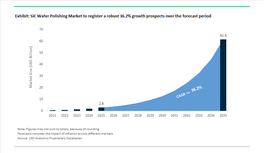
The SiC wafer polishing market (USD 2.8 billion in 2025, expanding at a 36.2% CAGR to USD 61.5 billion by 2035) has become a strategic bottleneck-and value lever-within the wide bandgap semiconductor supply chain. As power device manufacturers accelerate deployment of SiC MOSFETs and diodes for 800-V EV platforms, traction in rail traction, renewable inverters, and hyperscale power supplies, wafer surface quality now directly determines yield, die reliability, and total cost of ownership. Leading device manufacturers and substrate suppliers are converging on 200 mm SiC as the next industrial standard, with internal manufacturing roadmaps consistently indicating 30-40% cost-per-chip reduction potential driven by die-per-wafer scaling-provided polishing precision and subsurface integrity can be maintained at scale.
The core structural shift reshaping demand is the move from mechanical finishing toward tightly controlled, multi-step chemical mechanical polishing (CMP) architectures specifically engineered for hard, brittle SiC crystal systems. Unlike 150 mm production, 200 mm wafers impose significantly tighter flatness, total thickness variation (TTV), and subsurface damage (SSD) thresholds to avoid gate oxide reliability failures and premature breakdown in high-field devices. As a result, manufacturers are prioritizing polishing platforms capable of achieving surface roughness below 0.5 nm Ra while suppressing micro-crack propagation introduced during grinding and lapping. CMP consumables-pads, diamond-based slurries, and post-CMP cleaning chemistries-have moved from commodity inputs to yield-critical technologies, with polishing time, defectivity, and SSD depth now treated as first-order economic variables in fab cost models.
This substitution logic is clear across EV and industrial power electronics: higher-voltage architectures demand defect-free drift layers and ultra-smooth surfaces to sustain higher electric fields without compromising device lifetime. Poor polishing translates directly into higher leakage, lower breakdown voltage, and yield loss-outcomes that negate the cost advantages of 200 mm substrates. Conversely, advanced polishing processes improve die yield, reduce downstream epitaxy defects, and shorten overall cycle time, delivering measurable gains in wafer throughput and fab utilization. These dynamics are reinforcing rapid capacity build-out of polishing and CMP infrastructure alongside new SiC crystal growth and epitaxy investments, particularly as North America and Europe pursue localized wide-bandgap semiconductor corridors to reduce reliance on Asian supply chains.
Market Analysis: Strategic Developments Transforming the Sic Wafer Polishing Landscape
The SiC Wafer Polishing market experienced significant acceleration across funding activity, product innovation, and regional capacity expansions. A landmark development occurred in December 2025, when Wolfspeed secured a USD 698.6 million Section 48D tax refund, strengthening its capital base for 200 mm SiC wafer expansion and advancing its U.S. “Silicon Carbide Corridor.” This initiative substantially increases domestic substrate output and directly boosts demand for corresponding CMP slurries, diamond abrasives, and high-uniformity polishing pads. Earlier in June 2025, a strategic joint development agreement between a U.S. CMP consumables provider and a Japanese semiconductor equipment leader signaled a coordinated industry push to create SiC-specific slurry chemistries with higher Material Removal Rates (MRR) and lower SSD-core metrics for 200 mm wafer readiness.
Japan intensified its leadership in equipment innovation with the May 2025 launch of new Electrochemical-Mechanical Polishing (ECMP) systems optimized for SiC, enabling reduced process chemical consumption and improved surface flatness. This supports sustainability requirements while maintaining atomic-level material control. On the other hand, U.S. fabs began qualification runs for 200 mm SiC substrates in April 2025, triggering a noticeable spike in orders for low-defect CMP slurries and high-purity pads, confirming broad industry alignment behind the wafer transition. In January 2025, Wolfspeed’s Gen 4 MOSFET platform launch reinforced the importance of premium-quality polished substrates, as high-power applications require minimal crystalline defects to achieve breakthrough efficiency and thermal performance.
Throughout 2024, global process technology advancements supported the transition toward higher yield and die density. In December 2024, X-FAB’s XbloX SiC MOSFET process upgrade highlighted reliance on advanced planarization to support reduced cell pitch and maximize die-per-wafer output. Complementing this, May 2024 saw the creation of a strategic material alliance between Soitec and Tokai Carbon to secure polycrystalline SiC feedstock for Soitec’s SmartSiC™ platform-an upstream milestone enabling downstream polishing consistency. The Asia-Pacific region also emerged as a significant new demand center with India announcing its first SiC semiconductor plant in March 2024, scheduled to begin epitaxy wafer production by December 2025, anchoring regional adoption of polishing solutions tied to SiC device fabrication.
SiC Wafer Polishing Market Trends and Opportunities
Trend 1: Transition to Onsite, Integrated Polishing for 200mm Wafer Production
Leading SiC IDMs are internalizing polishing to manage the mechanical fragility and uniformity demands of 200mm wafers, which deliver ~2.25× more die area than 150mm substrates but amplify sensitivity to Total Thickness Variation (TTV), bow, and subsurface damage.
In April 2025, STMicroelectronics detailed its €5 billion SiC Campus in Catania, Italy—one of the first fully integrated European facilities spanning substrate engineering, polishing, epitaxy, and device fabrication. Designed to scale toward 15,000 wafers per week by 2033, the campus embeds onsite 200mm polishing to close feedback loops between crystal growth defects and CMP outcomes, reducing breakage risk and variability inherent in outsourced logistics.
Similarly, Wolfspeed formally launched its 200mm SiC materials portfolio in September 2025, standardizing wafers at ~350 μm thickness. By integrating boule growth and polishing, Wolfspeed has reported meaningful reductions in micropipe density (MPD) and threaded screw dislocations (TSDs)—defects that disproportionately impact high-voltage MOSFET yields.
onsemi reinforced this trend by confirming 200mm substrate qualification for revenue production in 2025, supported by a €2 billion expansion in the Czech Republic. Its vertically integrated “substrate-through-fab” model is explicitly designed to eliminate contamination and handling risks associated with third-party polishing—an increasingly unacceptable variable at 200mm scale.
Trend 2: Defect-Specific Polishing to Suppress Basal Plane Dislocations (BPDs)
As device architectures evolve, polishing strategies are becoming defect-aware rather than planar-only, targeting the suppression of basal plane dislocations that trigger stacking faults and body diode degradation in SiC MOSFETs.
Studies published across 2024–2025 confirm that pre-CMP subsurface damage (SSD) typically extends 2–5 μm beneath the surface—deep enough to seed BPD propagation if not carefully removed. Modern CMP platforms are now engineered to balance chemical oxidation and mechanical action, achieving material removal rates (MRR) of ~100–500 nm/h while holding Ra below 0.25 nm, a threshold increasingly demanded by epitaxy teams.
Academic work published in October 2025 showed that BPD-induced stacking faults remain the dominant long-term failure mechanism in 4H-SiC drift regions. Advanced polishing and ion-assisted techniques have demonstrated reductions in total dislocation density to ~2.3×10⁷ cm⁻², with BPD densities lowered to ~3.3×10⁶ cm⁻² on 6-inch n-type wafers—levels that materially improve device lifetime under high-current stress.
To cope with SiC’s extreme hardness—where MRRs are 30–50% lower than silicon—tool suppliers are embedding AI-driven spark detection, slurry chemistry analytics, and coolant monitoring. These systems dynamically adjust pressure and chemistry to prevent the introduction of new threading edge dislocations (TEDs) during aggressive material removal, aligning polishing outcomes with device-reliability targets rather than throughput alone.
Opportunity 1: CHIPS Act–Driven Capital Influx and Onshored Polishing Capacity
The U.S. CHIPS and Science Act has catalyzed a step-change in domestic SiC investment, with polishing emerging as a priority capability to secure EV and defense supply chains.
In October 2024, the U.S. Department of Energy finalized a $544 million ATVM loan to SK Siltron CSS for expansion of its Bay City, Michigan facility. The site is being positioned among the top global producers of automotive-grade SiC wafers by 2027, with advanced polishing at the core of yield and reliability targets.
This was reinforced by a $300 million State of Michigan investment announced in September 2025 to accelerate high-volume wafer output, leveraging polishing IP developed at SK Siltron’s Auburn, Michigan R&D center.
At the federal level, the U.S. Department of Commerce announced $210 million in direct funding in December 2025 for semiconductor materials and critical minerals processing. These incentives are explicitly designed to reduce the ~95% concentration of downstream assembly and packaging in the Indo-Pacific, creating sustained demand for U.S.-based, high-spec polishing infrastructure.
Opportunity 2: Double-Sided Polishing (DSP) for Vertical and Double-Side–Cooled SiC Devices
The industry’s shift toward trench MOSFETs, vertical architectures, and double-side–cooled power modules is creating a specialized requirement for wafers polished on both the Si-face and C-face.
A 2025 study on double-side–cooled SiC modules showed that dual-polished substrates reduce thermo-mechanical stress by ~50%, materially improving solder joint reliability and power cycling endurance. This architecture is rapidly becoming standard for high-performance EV inverters, where both surfaces must support silver sintering and low-resistance interconnects.
Technically, this is non-trivial: the C-face polishes at different rates than the Si-face, historically limiting backside epitaxy. Recent DSP CMP processes have achieved sub-nanometer roughness on both faces, enabling backside epitaxial growth critical for vertical JFETs and advanced MOSFET designs that optimize carrier mobility along the c-axis.
From a manufacturing standpoint, advanced double-side grinding and polishing tools are gaining traction in 200mm fabs to minimize warp and TTV. By removing material symmetrically, DSP reduces residual stress that would otherwise lead to wafer breakage during high-temperature anneals—directly translating into higher usable wafer yields and lower scrap rates.
Market Share Analysis: SiC Wafer Polishing Market
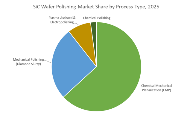
Market Share by Process Type: Chemical Mechanical Planarization (CMP) Sets the Yield and Scaling Benchmark
Chemical Mechanical Planarization (CMP) commands around 60% of the SiC wafer polishing market because it is the only process that consistently delivers epi-ready, damage-free surfaces at production scale—an absolute requirement as SiC manufacturing migrates from pilot lines to automotive-grade fabs. The economic logic behind CMP’s dominance is increasingly clear in 2025: next-generation single-wafer CMP chemistries now achieve material removal rates of 8–10 µm/hour, unlocking up to a 10× throughput improvement versus legacy mechanical polishing and directly addressing the industry’s biggest bottleneck—SiC wafer cost. Further, CMP’s ability to reach sub-angstrom (<0.1 nm) surface roughness eliminates subsurface damage, which is the primary root cause of early breakdown and yield loss in high-voltage devices. This capability becomes non-negotiable as the market transitions to 200 mm (8-inch) SiC wafers, where wafer bow and warp amplify defect risks that only CMP can uniformly correct. From a cost perspective, the rapid adoption of closed-loop slurry delivery systems—cutting consumable usage by 30–50%—has shifted CMP from a perceived “premium” step to the most cost-efficient route at scale. As fabs chase higher yields, larger wafers, and lower cost of ownership, CMP has effectively become the process standard that defines manufacturability in the SiC wafer polishing ecosystem.
Market Share by Application: Power Electronics Drive Precision Demand at Automotive Scale
Power electronics account for approximately 70% of total SiC wafer polishing demand, reflecting how tightly polishing quality is now linked to performance, reliability, and economics in EVs and energy infrastructure. The surge is led by SiC MOSFETs, which alone are expected to represent about 42% of the total SiC device mix in 2025, and which impose the most stringent surface requirements due to their high-frequency switching and thermal loading profiles. The industry-wide shift to 800V EV architectures has further entrenched this dominance: perfectly planarized wafers are essential to sustain the higher electric fields without premature breakdown, making polishing quality a gatekeeper for OEM qualification. Superior polishing also delivers tangible downstream value—leading manufacturers report that defect-free CMP surfaces enable up to 30% reductions in chip area, improving die-per-wafer economics and accelerating adoption across traction inverters and onboard chargers. Beyond mobility, renewable energy applications, particularly 1500V DC solar and grid inverters, are scaling rapidly and require ultra-low-defect SiC substrates to guarantee 25-year field lifetimes under thermal and electrical stress. Taken together, the combination of automotive electrification, high-voltage power density targets, and long-life energy infrastructure has made power electronics the structural demand anchor for the SiC wafer polishing market—cementing its 70% share and shaping investment priorities across the polishing value chain.
Competitive Landscape: Market Leaders Shaping Sic Wafer Polishing Technology and Supply Chains
The competitive landscape of the SiC Wafer Polishing market is defined by companies capable of delivering low-defect substrates, precision CMP slurries, advanced abrasives, and integrated process controls. As the industry moves to 200 mm wafers and EV power electronics proliferate, differentiation increasingly hinges on SSD minimization, particle size uniformity, high MRR capability, and sustainability-driven process innovation. Leading companies are investing in material science, end-to-end supply chain integration, and next-generation CMP technologies to meet the performance requirements of Wide Bandgap power semiconductors.
Wolfspeed, Inc. - Driving The Global Transition To 200 Mm Sic Substrates
Wolfspeed remains the global leader in vertically integrated SiC technology, pioneering the volume production of 200 mm SiC wafers, which form the backbone of next-generation power electronics. Its expanding U.S. “Silicon Carbide Corridor” strengthens domestic supply sovereignty and ensures the reliable availability of high-quality substrates for EV powertrain and industrial applications. Wolfspeed’s substrate and epitaxy innovations are widely adopted by Tier-1 automotive OEMs such as Toyota, reflecting superior device reliability. The company’s deep investment in defect reduction and SSD control improves yield performance significantly, positioning Wolfspeed at the forefront of SiC polishing demand and ecosystem leadership.
Resonac Holdings - Global Leader in Epi-Wafers and Advanced CMP Slurry Engineering
Resonac (formerly Showa Denko) plays a central role in the SiC wafer ecosystem through its mass production of 6-inch wafers and sampling of 200 mm epi-wafers, ensuring early availability of large-diameter substrates. Its CMP slurry portfolio is engineered with breakthrough nano-scale Particle Design Technology that balances high MRR with ultra-low scratch profiles, making it indispensable for hard SiC surfaces. Resonac’s sustainability-driven R&D-such as the July 2025 CO₂-based SiC powder project-demonstrates its commitment to cost-efficient and eco-efficient material supply. Its broad range of polishing particles positions the company as a top-tier supplier to global CMP workflows.
Coherent Corp. - High-Performance Sic Substrates For RF, 5G and Power Electronics
Coherent is a critical supplier for semi-insulating SiC substrates used in GaN-on-SiC RF amplifiers, a foundational technology for 5G infrastructure. It manufactures wafers up to 200 mm, supporting the industry’s shift toward larger, cost-efficient substrates with improved yield. Coherent’s epitaxy solutions shorten device manufacturers’ development cycles and require exceptionally polished wafer surfaces to achieve high-frequency performance consistency. Serving EV, aerospace and high-temperature electronics markets, Coherent is strongly positioned within the premium segment of SiC polishing demand.
Fujimi Corporation - Specialist in Diamond Abrasives and CMP Consumables For Sic
Fujimi stands out for its expertise in advanced abrasives, offering diamond-based CMP slurries and highly refined powders essential for effective SiC material removal given its exceptional hardness. Its products support multi-layer semiconductor fabrication, and the company maintains a wide global footprint with revenue contributions from North America (24%), Taiwan (20%) and China (15%). Fujimi's R&D efforts prioritize uniform MRR and minimized SSD-key challenges unique to Wide Bandgap substrates-making its materials indispensable in next-generation SiC polishing processes.
Entegris, Inc. - Global Leader in High-Purity CMP Materials and Contamination Control
Entegris provides a comprehensive suite of CMP consumables-including diamond, colloidal silica and hybrid slurry formulations-optimized for the demanding polishing steps in SiC wafer fabrication. Its advanced filtration systems are designed to eliminate contamination risks that could compromise polished Low-Defect Substrates. With strong integration across deposition, cleaning and critical materials handling, Entegris enables end-to-end quality assurance for SiC fabs. The company’s strategic expansions across Asia-Pacific, North America and Europe align directly with the global build-out of power electronics and 200 mm SiC capacity.
The United States is positioning 200 mm (8-inch) SiC wafer polishing as a strategic bottleneck technology under the CHIPS and Science Act, recognizing surface finish quality as a yield-defining step for power semiconductors. In December 2025, the U.S. Department of Commerce allocated USD 210 million in direct incentives to companies involved in advanced material processing, explicitly including ultra-precision polishing, CMP consumables, and in-line metrology for SiC substrates. This funding is designed to accelerate domestic readiness for high-volume 8-inch wafer qualification while reducing reliance on offshore finishing expertise.
A central anchor of this strategy is Wolfspeed, which ramped its Mohawk Valley Fab in mid-2025 as the world’s first fully automated 200 mm SiC fabrication facility. The site integrates next-generation polishing modules with AI-enabled surface inspection, achieving sub-2 nm RMS surface roughness—a critical threshold for high-voltage MOSFET reliability. Parallel to device fabs, U.S. CMP consumable suppliers announced capacity expansions for diamond abrasives and SiC-specific slurries in June 2025, reflecting the rapid scale-up of domestic EV traction inverter demand.
China: 50% Semiconductor Equipment Self-Sufficiency and CMP Localization
China’s SiC wafer polishing strategy is tightly aligned with its “Dual Circulation” policy, which prioritizes domestic substitution of advanced semiconductor equipment. According to the March 2025 Government Work Report, Beijing is targeting 50% self-sufficiency in semiconductor equipment by end-2025, with SiC CMP and ultra-precision grinding identified as high-priority gaps. This focus is particularly acute for 8-inch SiC wafers, where polishing complexity and tool IP have historically favored foreign suppliers.
Domestic champions such as Hwatsing and AMEC reported technical breakthroughs in 200 mm SiC polishing platforms, enabling tighter control of subsurface damage (SSD) and wafer bow. These advances are backed by aggressive state financing: in 2025, government-backed industrial guidance funds deployed approximately CNY 400 billion (~USD 56 billion) into high-tech manufacturing, with third-generation semiconductors receiving a significant allocation. As export controls persist, China’s ability to localize CMP tools and consumables is becoming a decisive factor in its SiC power device roadmap.
South Korea: Yongin Megacluster and Compound Semiconductor Diversification
South Korea is extending its memory-centric semiconductor dominance into compound semiconductors, supported by a KRW 700 trillion (~USD 534 billion) long-term investment plan. In December 2025, the government confirmed that the Yongin Semiconductor Megacluster will incorporate dedicated SiC and GaN lines, positioning polishing and wafer finishing as shared infrastructure assets rather than isolated process steps.
A major milestone came in November 2025, when SK Keyfoundry completed the integration of SiC mass-production capabilities, targeting 1200 V SiC MOSFET foundry services by early 2026. Recognizing talent scarcity in ultra-precision processes, policymakers raised R&D tax credits to 50% for companies working on advanced metrology, CMP modeling, and polishing verification for wide-bandgap substrates. This approach links fiscal policy directly to polishing yield improvement, reinforcing South Korea’s ambition to become a regional SiC foundry hub.
Japan: GX 2040 and Low-Chemical Polishing Innovation
Japan is leveraging its legacy strength in precision equipment and materials science to redefine SiC wafer polishing under the Green Transformation (GX) 2040 Vision, approved by the Cabinet on January 18, 2025. The policy explicitly supports low-chemical-consumption and low-environmental-impact polishing technologies, aligning sustainability goals with semiconductor competitiveness.
In May 2025, Japanese toolmakers introduced Electrochemical-Mechanical Polishing (ECMP) systems specifically engineered for SiC wafers. By softening the surface electrochemically prior to mechanical removal, ECMP significantly reduces slurry usage, abrasive wear, and subsurface damage, addressing both cost and ESG pressures. Vertically integrated players such as Resonac and ROHM are expanding wafer-to-device production lines to secure domestic 200 mm polishing capacity, supporting large-scale deployment of SiC devices in solar inverters exceeding 3.8 GW and next-generation EV powertrains.
Italy: Catania as Europe’s Integrated SiC Polishing Hub
Italy has emerged as Europe’s flagship location for SiC manufacturing, anchored by a fully integrated approach supported by the EU Chips Act. In June 2024, with momentum extending through 2025, STMicroelectronics unveiled plans for its €5 billion Catania mega-fab, designed as a closed-loop SiC ecosystem spanning crystal growth, wafer slicing, polishing, epitaxy, and testing.
This facility—expected to reach 15,000 wafers per week by 2033—places ultra-precision polishing at the center of Europe’s automotive electrification strategy. As European OEMs migrate toward 800 V EV architectures, polishing quality becomes critical to device reliability and switching efficiency. The Catania hub represents the largest SiC capacity ever announced in Europe, making Italy a strategic node for surface-finish excellence and regional supply-chain sovereignty.
Thailand: Emerging Southeast Asian Back-End Polishing Node
Thailand is positioning itself as a cost-competitive back-end and finishing hub for SiC devices within Southeast Asia. In September 2024, the Thailand Board of Investment (BOI) approved USD 350 million in funding for a joint venture between Hana Microelectronics and PTT. The project focuses on back-end processing and finishing of SiC power semiconductors, including polishing-adjacent steps critical to device packaging reliability.
By targeting finishing rather than boule growth, Thailand is integrating into regional EV and renewable energy supply chains without competing directly with upstream crystal suppliers. This strategy allows the country to capture value in precision polishing, inspection, and packaging, reinforcing ASEAN’s role in the global SiC ecosystem.
2025 Strategic Matrix: SiC Wafer Polishing Market by Country
SiC Wafer Polishing Market Strategic Matrix
|
Country
|
Strategic Driver
|
2025 Key Milestone
|
Primary Polishing Technology Focus
|
|
United States
|
CHIPS Act reshoring
|
USD 210 M materials & polishing incentives
|
200 mm automated CMP with AI metrology
|
|
China
|
Equipment self-sufficiency
|
50% localization target by end-2025
|
Domestic CMP tools & slurry development
|
|
South Korea
|
Yongin Megacluster
|
KRW 700 T future chip investment
|
Foundry-scale SiC MOSFET polishing
|
|
Japan
|
GX 2040 green tech
|
ECMP commercialization (May 2025)
|
Low-slurry, low-SSD polishing
|
|
Italy
|
EU Chips Act
|
ST Catania integrated SiC hub
|
Boule-to-wafer precision polishing
|
|
Thailand
|
BOI incentives
|
USD 350 M Hana-PTT JV
|
Back-end SiC finishing & inspection
|
SiC Wafer Polishing Market Report Scope
SiC Wafer Polishing Market
|
Parameter
|
Details
|
|
Market Size (2025)
|
$2.8 Billion
|
|
Market Size (2035)
|
$61.5 Billion
|
|
Market Growth Rate
|
36.2%
|
|
Segments
|
By Process Type (Chemical Mechanical Planarization, Mechanical Polishing, Electropolishing, Plasma-Assisted Polishing, Chemical Polishing), By Product / Consumable Type (Polishing Slurries, Polishing Pads, Abrasive Powders, Conditioners & Cleaning Agents), By Wafer Size (2-Inch & 4-Inch, 6-Inch / 150 mm, 8-Inch / 200 mm, 12-Inch / 300 mm), By Application (Power Electronics, RF & Microwave Devices, Optoelectronics, Sensors & Detectors)
|
|
Study Period
|
2019- 2024 and 2025-2034
|
|
Units
|
Revenue (USD)
|
|
Qualitative Analysis
|
Porter’s Five Forces, SWOT Profile, Market Share, Scenario Forecasts, Market Ecosystem, Company Ranking, Market Dynamics, Industry Benchmarking
|
|
Companies
|
Entegris Inc., Applied Materials Inc., Fujimi Incorporated, Ferrotec Holdings Corporation, Coherent Corp., Kemet International Limited, Saint-Gobain S.A., JSR Corporation, Cabot Microelectronics, SK Siltron Co. Ltd., DuPont de Nemours Inc., Resonac Holdings Corporation, Okamoto Machine Tool Works Ltd., Axus Technology, Lapmaster Wolters GmbH
|
|
Countries
|
US, Canada, Mexico, Germany, France, Spain, Italy, UK, Russia, China, India, Japan, South Korea, Australia, South East Asia, Brazil, Argentina, Middle East, Africa
|
SiC Wafer Polishing Market Segmentation
By Process Type
- Chemical Mechanical Planarization (CMP)
- Mechanical Polishing
- Electropolishing
- Plasma-Assisted Polishing
- Chemical Polishing
By Product / Consumable Type
- Polishing Slurries
- Polishing Pads
- Abrasive Powders
- Conditioners & Cleaning Agents
By Wafer Size
- 2-Inch & 4-Inch
- 6-Inch (150mm)
- 8-Inch (200mm)
- 12-Inch (300mm)
By Application
- Power Electronics
- RF and Microwave Devices
- Optoelectronics
- Sensors and Detectors
By Region
- North America (United States, Canada, Mexico)
- Europe (Germany, France, United Kingdom, Spain, Italy, Rest of Europe)
- Asia Pacific (China, India, Japan, South Korea, Australia, Rest of APAC)
- South and Central America (Brazil, Argentina, Rest of SCA)
- Middle East and Africa (Saudi Arabia, UAE, South Africa, Rest of Middle East, Rest of Africa)
Top Companies in SiC Wafer Polishing Market
- Entegris, Inc.
- Applied Materials, Inc.
- Fujimi Incorporated
- Ferrotec Holdings Corporation
- Coherent Corp.
- Kemet International Limited
- Saint-Gobain S.A.
- JSR Corporation
- Cabot Microelectronics
- SK Siltron Co., Ltd.
- DuPont de Nemours, Inc.
- Resonac Holdings Corporation
- Okamoto Machine Tool Works, Ltd.
- Axus Technology
- Lapmaster Wolters GmbH
*- List not Exhaustive
