Diamond Wire Market Overview: Precision Slicing, Kerf-Loss Reduction & Next-Gen Tungsten Core Technologies Driving Global Manufacturing Efficiency
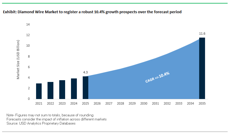
The Diamond Wire Market, valued at USD 4.3 billion in 2025 and projected to reach USD 11.6 billion by 2035 at a strong 10.4% CAGR, is accelerating due to the industry-wide transition to fixed abrasive diamond wire sawing (DWS) across PV solar wafering, semiconductor manufacturing, and wide-bandgap substrate production. As manufacturers push for ultra-thin wafer slicing, minimal kerf loss, and higher throughput, diamond wire has become the essential consumable driving both cost-per-watt reductions in solar modules and yield improvements in SiC/GaN power electronics. With the shift away from legacy slurry-based abrasive sawing now nearly complete, DWS stands as the universal global standard for high-precision, high-volume slicing of silicon, sapphire, SiC, and other advanced substrates.
Market momentum is increasingly shaped by wire diameter evolution (40 μm → 36 μm → 32 μm), high-strength tungsten alloy cores offering superior breaking and torsional resistance, and optimized abrasive retention critical for wafer quality and Total Thickness Variation (TTV) control. As PV manufacturers race to reduce polysilicon consumption and SiC fabs scale 150 mm and 200 mm wafer production, procurement teams and OEMs are prioritizing wire uniformity, mechanical stability, abrasive wear behavior, and lifecycle predictability. Through 2035, diamond wire technology will remain at the center of global cost competitiveness in solar and advanced semiconductor manufacturing, making high-precision slicing capability a strategic differentiator for the entire clean energy and electronics value chain.
Market Analysis: Technology Shifts, Tungsten Wire Adoption, and Advanced Slicing Breakthroughs
The Diamond Wire Market is experiencing rapid transformation as advanced slicing requirements reshape the competitive landscape. February 2025 marked a critical milestone: industry sources confirmed that the transition from slurry-based LAS to fixed abrasive DWS in the PV sector reached nearly 100% completion, sealing diamond wire’s role as the standard for global solar wafer slicing. As polysilicon prices stay elevated, manufacturers increasingly adopt tungsten-core diamond wire, with several top-tier PV wafer plants reporting higher efficiency and lower kerf-loss in early 2025. This shift is reinforced by research findings in August 2025, confirming that wafer quality (especially TTV) is optimal during the stable wear period of diamond wire, guiding quality assurance and wire replacement schedules.
The semiconductor segment is undergoing parallel innovation. In September 2025, researchers published findings that highlight the urgent need for advanced vibration-control strategies in SiC slicing, as lateral vibration increases fracture risk in thin wafers. Additionally, academic studies in late 2024 demonstrated the successful cutting of single-crystal diamond substrates using metal-bonded fixed diamond grain wire, achieving exceptional grit fixation strength (800 MPa). This breakthrough underscores diamond wire’s expanding role beyond silicon into next-generation power devices and even diamond substrate fabrication for quantum and high-power applications.
Meanwhile, the upstream and equipment side is consolidating. September 2025 saw Sumitomo Electric’s subsidiary A.L.M.T. complete an acquisition to strengthen its diamond die and core wire capabilities, reinforcing vertical control over wire drawing technologies essential for DWS. Capacity growth continues across Asia, with a major producer expanding diamond wire production by 15% in Q4 2024 to meet Southeast Asia’s rapidly expanding PV manufacturing base. These developments collectively indicate a market moving toward ultra-thin wafers, tungsten innovation, material diversification, and high-volume global supply capability.
Trends and Opportunities Reshaping High-Precision Slicing and Sustainable Manufacturing in the Diamond Wire Market
Trend 1: Shift to Ultra-Thin Diamond Wire (≤50 µm) as Solar Manufacturers Prioritize Kerf Reduction and High-Yield Wafering
A core trend driving the diamond wire market is the industry's transition toward ultra-thin diamond wire, typically in the 35–50 µm range, engineered with fine diamond grit to dramatically reduce kerf loss in silicon wafer slicing. The shift is tightly correlated with the solar sector’s need to decrease cost per watt while simultaneously increasing cell efficiency.
The industry-wide movement from slurry-based multi-wire saws, which traditionally produced kerf losses of 200 µm or more, to fixed abrasive diamond wire sawing (DWS) initially reduced kerf loss to 150–170 µm. The newest generation of ultra-thin diamond wires aims to push kerf loss well below this range, directly improving material utilization for monocrystalline silicon.
The economic incentive is substantial: thinning wafers from 160 µm to 50 µm could reduce module manufacturing cost by approximately USD 0.07/W, accelerating the downward trajectory of solar LCOE. In addition, DWS unlocks remarkable throughput advantages—producing 13,800 wafers/day from a standard 156 mm × 156 mm ingot section, more than double the output of older loose abrasive slurry systems (6,500 wafers/day). This performance uplift explains the near-universal adoption of DWS across the global PV supply chain, especially in China, where large-scale PERC, TOPCon, and HJT cell lines increasingly depend on ultra-thin wires.
Trend 2: Semiconductor Industry Qualification of Diamond Wire for Precision Slicing of SiC, GaN, Sapphire, and Hard-Crystal Substrates
As semiconductor devices migrate to wide-bandgap materials (SiC, GaN) and high-value substrates (sapphire), diamond wire sawing is rapidly replacing legacy inner-diameter (ID) saws. This shift is driven by DWS’ ability to achieve superior dimensional accuracy, surface quality, and material yield.
Diamond multi-wire systems have demonstrated the ability to halve cutting time for 4-inch sapphire ingots, significantly enhancing throughput. Precision metrics such as Total Thickness Variation (TTV) of 10 µm and bow (BOW) of 10 µm are now achievable using advanced DWS equipment, meeting the stringent tolerances required for SiC MOSFET, GaN HEMT, and high-frequency RF applications.
Kerf width is another strategic differentiator: DWS achieves 0.15–0.26 mm, compared to 0.300–0.500 mm for ID saws, reducing the loss of expensive materials like SiC and sapphire. Equally important is DWS’s elimination of slurry-based contamination, removing the need for PEG slurry recovery systems and significantly lowering hazardous waste generation—an increasingly relevant criterion for sustainability audits within semiconductor fabs.
Opportunity 1: High-Speed Diamond Wire for Monocrystalline Sapphire, Optical Crystals, and Specialty Ceramics
The growth of LEDs, smartphone cover glass, IR optics, and specialty piezoelectric devices creates a robust opportunity for diamond wire in slicing large-diameter sapphire boules and optical-grade crystals. These applications require a combination of high throughput, low subsurface damage (SSD), and minimal fracture risk—areas where diamond wire offers superior performance.
DWS supports wire travel speeds up to 1,500 meters/min, enabling rapid reciprocating cutting essential for processing large, high-purity boules. Minimizing SSD depth is crucial for reducing post-slicing polishing and CMP requirements, directly lowering overall manufacturing costs.
Diamond wire's controlled abrasive action also enables precise slicing of quartz, lithium niobate (LiNbO₃), lithium tantalate (LiTaO₃) and advanced technical ceramics. This minimizes cracking, enhances yield, and supports the rising demand for crystal materials used in RF filters, optical modulators, MEMS sensors, and high-performance optics.
Opportunity 2: Recycled Diamond Wire as a Strategic Enabler for Secondary Industries and Silicon Reclamation
With more than 150 million km of diamond wire consumed annually in the PV industry, a high-value circular economy opportunity is emerging for recycling worn wire and recovering embedded materials.
Even after diamond grit degradation, the core wire retains functional and monetary value. Recovered wires can be repurposed for low-precision applications such as stone quarrying, dimensional granite block cutting, rough concrete demolition, and others.
Simultaneously, kerf-loss silicon—historically considered waste—represents a new resource pathway. Studies show that kerf silicon powder can be purified and repurposed as a potential anode material for lithium-ion batteries, supporting the battery industry's push toward silicon-enhanced anodes.
A parallel development is the shift toward tungsten (W) core wire, which provides 1.2–1.3× greater breaking strength than high-carbon steel at equivalent gauges. This allows for the reliable manufacture of ultra-thin wires (<40 µm) for advanced wafering needs and increases the recycling value of spent consumables by circulating tungsten back into high-value metallurgical and additive manufacturing supply chains.
Diamond Wire Market Share Analysis
Market Share by Diamond Wire Type: Electroplated Diamond Wire Leads with 61.4% Share
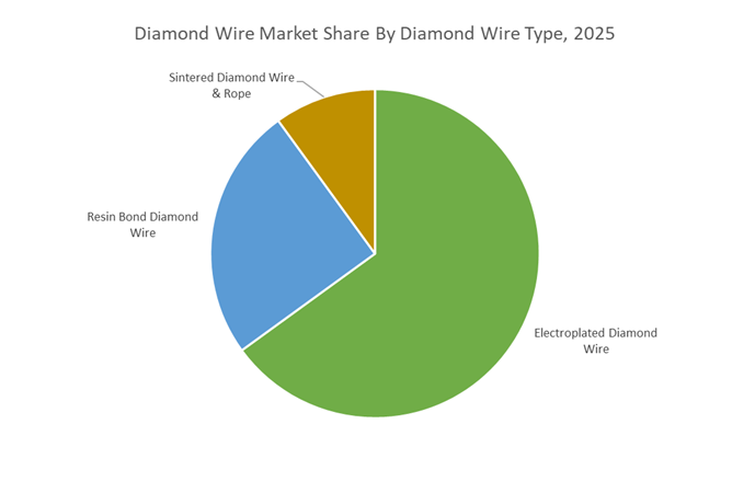
Electroplated Diamond Wire dominates the global Diamond Wire Market with a 61.4% share in 2025, reflecting its unmatched scalability and performance advantages in the high-volume solar photovoltaic (PV) industry. Its leadership is driven by the material’s ability to deliver faster cutting speeds, higher wafer yields, tighter kerf control, and dramatically improved environmental performance by eliminating slurry waste—factors that have made electroplated wire the indispensable standard for silicon ingot slicing in solar wafer production. This strong market share is reinforced by aggressive global solar capacity expansion, where gigawatt-scale manufacturing facilities rely on electroplated wire to reduce per-watt module costs and boost throughput. Beyond solar, the broader competitive landscape highlights differentiated roles for other wire types: resin bond diamond wires are rising as critical tools for cutting harder, brittle advanced materials such as silicon carbide (SiC), technical ceramics, and battery anode materials, where minimizing micro-cracks directly influences downstream device performance; sintered diamond wires and ropes cater to heavy-duty industrial and construction applications where durability outweighs precision. Collectively, the segmentation illustrates a performance-driven hierarchy where electroplated wire anchors mass-market volume, resin bond wire supports next-generation semiconductor and EV materials, and sintered solutions address high-wear industrial cutting environments.
Market Share by End-Use Industry: Renewable Energy (Solar PV) Leads with 72.1% Share
Renewable Energy—dominated by solar photovoltaic manufacturing—accounts for a commanding 72.1% share in 2025, making it the primary demand engine shaping the entire Diamond Wire Market. This leadership reflects the solar industry’s extraordinary scale and rapid global expansion, which depends heavily on diamond wire slicing to improve wafer uniformity, reduce silicon loss, and meet aggressive cost-reduction targets under competitive module pricing pressures. Diamond wire sawing has become foundational to the production of monocrystalline and multicrystalline silicon wafers, the core building blocks of solar cells, and its widespread adoption has enabled the shift to thinner wafers that enhance module efficiency and reduce material usage. The dominance of the solar segment also accelerates R&D investment and manufacturing efficiency improvements, which subsequently benefit emerging high-value applications. Outside solar, electronics and semiconductor manufacturing represent the technology frontier, where cutting SiC, sapphire, and advanced ceramics demands precision, surface integrity, and reduced micro-damage—allowing resin bond and next-generation wire technologies to command premium pricing. Meanwhile, construction, infrastructure, and automotive applications form a stable but secondary revenue stream, leveraging diamond wires and ropes for heavy material cutting where wear resistance is crucial. Overall, the end-use segmentation underscores how the Diamond Wire Market is structurally tied to the global energy transition, with solar PV providing scale and semiconductors delivering technological advancement.
Country Analysis: Global Diamond Wire Market Innovation Hubs
China: PV Manufacturing Dominance Fueling Ultra-Fine Electroplated Diamond Wire Scale-Up
China remains the undisputed global center of demand and production for diamond wire cutting technology, driven by its overwhelming control of both silicon wafer manufacturing and global solar module production. With China accounting for over 95% of global wafer production and 86% of solar module output, the country is the anchor of high-volume adoption for electroplated diamond wire used in monocrystalline and polycrystalline silicon slicing. In 2025, more than 85% of PV cell manufacturing lines in China deployed electroplated saw wire, accelerating large-scale domestic investments in ultra-fine diamond wire below 80 µm, enabling sub-160-micron wafers essential for TOPCon, PERC, and emerging n-type cell architectures.
Government-driven expansion in solar installations—supported by the CPIA’s increased 2025 solar installation forecast of 270–300 GW AC—ensures long-term structural demand for diamond wire to process rising polysilicon and wafer volumes. Even temporary production cuts in early 2025, driven by market oversupply, did not diminish the underlying technical shift toward thinner wafers and lower kerf-loss cutting, both of which require more durable, consistent, and ultra-fine wire. Meanwhile, China’s 26% year-on-year increase in wafer exports in H1 2025—supporting new module assembly operations in countries like India and Indonesia—strengthens China’s centrality to the global diamond wire ecosystem. These dynamics establish China as the fastest-evolving and highest-volume market for advanced diamond wire slicing technologies.
Japan: Ultra-Fine Precision Diamond Wire and Semiconductor Specialty Applications
Japan continues to be a global leader in precision diamond wire manufacturing, specializing in ultra-fine, high-tensile wires used in semiconductor, LED, and sapphire substrate slicing. Japanese suppliers produce electroplated diamond wires as thin as sub-60 µm, engineered for the strict tolerances required in high-purity silicon wafers, sapphire substrates, WBG semiconductor materials, and other brittle, high-value materials. Leading manufacturers such as Asahi Diamond operate advanced production lines in Japan and Thailand, delivering wires that can exceed 3,200 MPa tensile strength, enabling high-speed slicing with exceptional reliability and minimal breakage.
Japan’s innovation ecosystem works closely with academic institutions to refine ultrasonic vibration-assisted diamond wire sawing and other advanced processing techniques aimed at reducing subsurface damage, kerf loss, crack propagation, and surface roughness when cutting extremely hard materials like SiC and sapphire. Companies like Nakamura Choukou export more than 38% of their ultra-fine wire output to high-growth semiconductor hubs in China and South Korea, solidifying Japan’s leadership in premium, high-precision diamond wire for advanced electronics manufacturing. The market’s specialization in ultra-fine, high-accuracy wires positions Japan at the forefront of next-generation wafer slicing technologies.
United States: Strategic Diamond Wire Adoption for SiC Wafer Slicing and Kerf-Loss Reduction
The U.S. diamond wire market is shaped by its national priority to domesticate the Silicon Carbide (SiC) supply chain for electric vehicles, defense, industrial drives, and power electronics. SiC is significantly harder than silicon, making diamond wire indispensable for slicing ingots into wafers. The rapid scaling of wafer manufacturing capacity by U.S.-based companies—such as Wolfspeed and Onsemi—is driving strong demand for specialized diamond wires engineered for high wear resistance, consistent abrasive exposure, and minimal wire deformation during SiC slicing.
However, SiC’s extreme hardness results in kerf losses exceeding 150 µm per wafer, a major cost burden for WBG semiconductor production. U.S. research institutions are therefore leading efforts to develop low-kerf diamond wire saw technologies, optimize abrasive distribution, and minimize the modification layer that forms during cutting. Parallel R&D into hybrid slicing approaches—such as laser-assisted SiC wafer slicing combined with diamond sawing—aims to reduce modification layers to as low as 16.5 µm, lowering material loss and improving wafer yield. These initiatives firmly position the United States as a high-innovation market focused on material efficiency, semiconductor competitiveness, and advanced diamond wire engineering.
Germany/Europe: Resin-Bonded Diamond Wire Advancements for Specialty Ceramics, Optics, and E-Mobility Materials
Europe is strengthening its position in specialty diamond wire solutions, particularly in resin-bonded diamond wire, which offers softer cutting action and greater flexibility for delicate or highly engineered materials. German and European manufacturers have expanded resin wire capacity by over 25% in the past year, driven by fast-expanding applications in EV battery components, advanced optics, lithium-based ceramics, and precision glass manufacturing. These sectors increasingly rely on resin-bonded wires to achieve reduced chipping, enhanced cut stability, and superior control when slicing brittle or high-value materials.
Companies such as TYROLIT exemplify Europe’s technical leadership, offering advanced electroplated and resin-bonded wire formulations designed for prolonged tool life and high cutting consistency under industrial conditions. Europe’s broader industrial ecosystem—covering e-mobility, aerospace materials, and specialty optical components—demands high-precision, low-damage slicing processes, making resin wires a central technology for next-generation manufacturing workflows. This positions Europe as a hub for niche, high-value diamond wire innovations that complement high-volume applications concentrated in Asia.
Competitive Landscape: Leading Suppliers Driving High-Precision Diamond Wire Sawing Innovations
The competitive landscape is defined by super-abrasive specialists, high-volume PV wire manufacturers, and legacy slicing-technology pioneers. Success is increasingly determined by suppliers’ ability to deliver precise electroplating, thin-diameter control, tungsten core wire engineering, and compatibility with multi-wire sawing systems for silicon, SiC, GaN, and sapphire wafers.
Asahi Diamond Industrial Co. Ltd. - Specialist in ultra-precise electroplated diamond wire for SiC and sapphire slicing
Asahi Diamond remains a global leader in super-abrasive tools with deep expertise in diamond wire engineered for hard, brittle semiconductor substrates. The company focuses on precision cutting solutions tailored to extremely strict TTV requirements essential for SiC and GaN power electronics. Its high grit-retention electroplated wires and tight diameter tolerance support highly stable multi-wire sawing, enabling manufacturers to achieve consistent wafer flatness and minimal microcracking.
Nanjing Sanchao Advanced Materials Co. Ltd. - High-volume supplier powering global PV wafer manufacturing
Nanjing Sanchao is one of the world’s highest-volume producers of diamond wire for the PV sector, supporting major wafer giants such as LONGi and TCL Zhonghuan. Its core strategy focuses on improving coating uniformity to prevent micro-wire breakage during high-speed slicing. The company’s scalability and process stability are instrumental in enabling ultra-thin PV wafers and lowering cost-per-watt across global solar markets.
Huari (Henan Yicheng New Energy Co. Ltd.) - Innovator in tungsten-core diamond wire for reduced kerf loss
Huari invests heavily in producing thinner core wires, including high-strength tungsten-core diamond wire, addressing industry demands for greater material savings amid fluctuating polysilicon prices. Huari also advances slurry and cooling fluid formulations, optimizing MRR (Material Removal Rate) while protecting wafer surface quality. Its R&D supports both PV and stone-processing applications, with a growing focus on next-generation ultra-thin slicing.
Meyer Burger Technology AG - Pioneer of industrial diamond wire sawing technology
Meyer Burger pioneered the industrialization of Fixed Abrasive Slicing Technology (FAST) and its DW288 saw series revolutionized global PV wafer cutting. While the company now emphasizes heterojunction (HJT) module production, its legacy technologies remain central to the PV industry’s transition from slurry-based sawing to water-based DWS processes. Meyer Burger’s innovations laid the foundation for high-throughput, environmentally friendly slicing systems.
Sumitomo Electric Industries Ltd. - Strengthening upstream wire and core technologies for DWS
Sumitomo Electric, through its subsidiary A.L.M.T., deepens its presence in diamond dies and ultra-hard materials, essential for high-precision wire drawing used in diamond wire manufacturing. Its September 2024 acquisition expands upstream control, improving efficiency and tolerance precision for carbon steel and tungsten core wires. This level of integration allows superior consistency in final wire diameter-critical for wafer quality and slicing stability.
Diamond Wire Market
|
Parameter
|
Details
|
|
Market Size (2025)
|
$4.3 Billion
|
|
Market Size (2035)
|
$11.6 Billion
|
|
Market Growth Rate
|
10.4%
|
|
Segments
|
By Diamond Wire Type (Electroplated Diamond Wire, Resin Bond Diamond Wire, Sintered Diamond Wire, Diamond Wire Rope), By Application Material (Monocrystalline Silicon, Polysilicon, Silicon Carbide, Sapphire Substrates, Glass & Optical Materials, Hard Ceramics), By Wafer Size (150–166 mm, 182–210 mm, 150–200 mm, Ultra-Thin Wafers), By End-Use Industry (Renewable Energy, Electronics & Semiconductor Manufacturing, Construction & Infrastructure, Automotive), By Wire Diameter (Ultra-Fine Wire, Standard Wire, Coarse Wire)
|
|
Study Period
|
2019- 2024 and 2025-2034
|
|
Units
|
Revenue (USD)
|
|
Qualitative Analysis
|
Porter’s Five Forces, SWOT Profile, Market Share, Scenario Forecasts, Market Ecosystem, Company Ranking, Market Dynamics, Industry Benchmarking
|
|
Companies
|
Asahi Diamond Industrial Co. Ltd., Nakamura Choukou Co. Ltd., Tyrolit Schleifmittelwerke Swarovski K.G., Hubei Fotao Diamond Co. Ltd., Suzhou Sitong Group Co. Ltd., Sino-Crystal Diamond Co. Ltd., ILJIN Diamond Co. Ltd., Henan Huanghe Whirlwind Co. Ltd., Noritake Co. Limited, DIABU Diamond Tools, Element Six, Disco Corporation, ACCRETECH, Meyer Burger Technology AG
|
|
Countries
|
US, Canada, Mexico, Germany, France, Spain, Italy, UK, Russia, China, India, Japan, South Korea, Australia, South East Asia, Brazil, Argentina, Middle East, Africa
|
Diamond Wire Market Segmentation
By Diamond Wire Type
- Electroplated Diamond Wire
- Resin Bond Diamond Wire
- Sintered Diamond Wire
- Diamond Wire Rope
By Application Material
- Monocrystalline Silicon
- Polysilicon
- Silicon Carbide
- Sapphire Substrates
- Glass & Optical Materials
- Hard Ceramics
By Wafer Size
- 156 mm / 166 mm
- 182 mm / 210 mm
- 150 mm / 200 mm
- Ultra-Thin Wafers
By End-Use Industry
- Renewable Energy
- Electronics & Semiconductor Manufacturing
- Construction & Infrastructure
- Automotive
By Wire Diameter
- Ultra-Fine Wire (≤80 μm)
- Standard Wire (80–120 μm)
- Coarse Wire (>120 μm)
By Region
- North America (United States, Canada, Mexico)
- Europe (Germany, France, United Kingdom, Spain, Italy, Rest of Europe)
- Asia Pacific (China, India, Japan, South Korea, Australia, Rest of APAC)
- South and Central America (Brazil, Argentina, Rest of SCA)
- Middle East and Africa (Saudi Arabia, UAE, South Africa, Rest of Middle East, Rest of Africa)
Top Companies in the Diamond Wire Market
- Asahi Diamond Industrial Co., Ltd.
- Nakamura Choukou Co., Ltd.
- Tyrolit Schleifmittelwerke Swarovski K.G.
- Hubei Fotao Diamond Co., Ltd.
- Suzhou Sitong Group Co., Ltd.
- Sino-Crystal Diamond Co., Ltd.
- ILJIN Diamond Co., Ltd.
- Henan Huanghe Whirlwind Co., Ltd.
- Noritake Co., Limited
- DIABU Diamond Tools
- Element Six
- Disco Corporation
- ACCRETECH
- Meyer Burger Technology AG
*- List not Exhaustive
