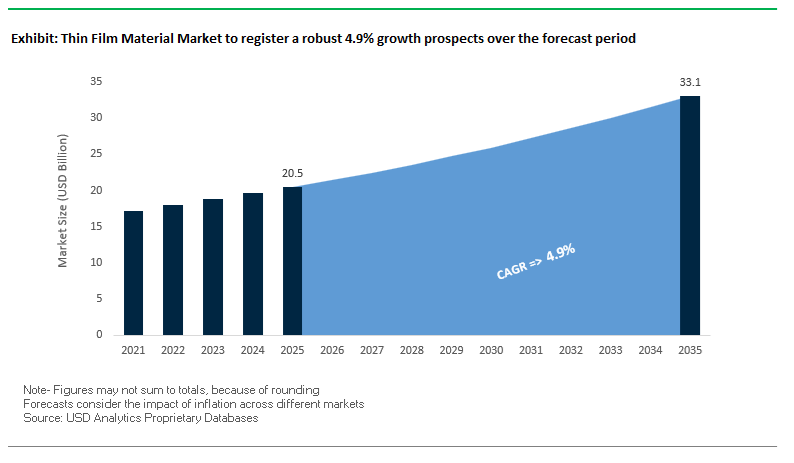
The Thin Film Material Market is valued at USD 20.5 billion in 2025, projected to reach USD 33.1 billion by 2035, growing at a steady CAGR of 4.9%. The market’s trajectory is tightly tied to the transformation of semiconductor architecture toward Gate-All-Around (GAA) transistors, 3D NAND, EUV lithography, Fan-Out Packaging, and high-density logic platforms.
The global thin-film materials industry is undergoing rapid expansion, driven by accelerated semiconductor fabrication investments, AI-driven computing demand, and intensified regionalization of chip supply chains. New fabrication nodes and advanced packaging approaches require chemically engineered, defect-free, and deposition-optimized thin films, pushing suppliers to expand capacity and introduce new chemistries.
A major catalyst came in December 2025, when Merck KGaA inaugurated its €500 million Semiconductor Solutions megasite in Kaohsiung, Taiwan, strengthening direct access to the world’s largest cluster of foundry manufacturers. The facility enhances Merck’s capabilities in ALD/CVD precursors and specialty gases, and is part of its broader €3 billion “Level Up” five-year program, which reached near-completion by November 2025. The ecosystem expansion ensures material consistency, accelerates innovation cycles, and improves regional supply chain resilience.
In the U.S., JX Nippon Mining & Metals continued aligning with domestic manufacturing initiatives by acquiring 260,000 m² of land in Arizona in November 2025, reinforcing its sputtering target production footprint. The strategic move responds directly to the rapid expansion of U.S. fabs supported by the CHIPS Act. Simultaneously, DuPont continued positioning itself at the center of advanced packaging workflows: in June 2025, it unveiled CYCLOTENE™ (DF-PID) for Fan-Out Panel-Level Packaging (FOPLP), enabling void-free Through-Glass Via (TGV) formation—an essential requirement for glass-core substrates targeting chiplet integration and high-density interposers. Earlier, in March 2025, DuPont highlighted the deployment of Microfill™ SFP-II-M copper plating chemistry engineered for large AI chip substrate uniformity, signaling direct support for HPC chip manufacturing. The company also reported a 58% reduction in Scope 1 and 2 emissions by February 2025, outpacing its SBTi commitments and reinforcing sustainability-driven procurement.
Industry-wide material innovation also accelerated. The early 2026 forecast indicates thin-film electrodes—especially carbon-based materials—will be the fastest-growing category due to their intrinsic flexibility, high surface area, and compatibility with next-gen wearable electronics. In October 2024, rising adoption of tantalum sputtering targets for corrosion-resistant coatings in surgical tools demonstrated increasing demand from medical applications, diversifying revenue beyond semiconductors. The shift shows how thin-film materials continue expanding into broader sectors including medical implants, optics, aerospace, and energy storage, supported by purity, adhesion, and microstructure control requirements.
Buyers and engineering decision-makers are increasingly prioritizing atomic-scale dimensional control, ultra-high-purity precursor chemistries, uniformity across large-area substrates, and high-throughput deposition to sustain Moore’s Law and the explosive growth of AI and HPC workloads. Thin film materials—ALD/CVD precursors, sputtering targets, dielectric films, and functional coatings—are strategic enablers of next-generation semiconductor scaling, power efficiency, and device reliability.
- Atomic-Layer Precision at Sub-10 nm Nodes- ALD technologies enable thickness control at 0.11 nm per cycle, essential for GAA FETs and ultra-thin high-k dielectrics.
- Ultra-High Purity Mandates (ppb–ppt Range)- Contaminants can induce dielectric breakdown and leakage, making ppb/ppt purity levels mandatory for leading-node DRAM and logic.
- Deposition Uniformity as Low as 0.15% Variation- Vital for large-area displays, photovoltaic coatings, and 300–450 mm wafers, ensuring reproducible optical/electrical output.
- Spatial ALD Throughput ≥ 60 nm/min- Addresses the fundamental bottleneck of ALD speed, enabling high-volume manufacturing (HVM) for memory and logic fabs.
- Materials Tailored for AI/ML and HPC Thermal Loads- Thin-film thermal management and barrier layers are central to chip reliability as power densities increase.
Breakthrough ALD Films, Cadmium-Free Quantum Dots, UWBG Epitaxy, and Ferroelectric HfO₂ Drive Next-Generation Thin Film Material Market Expansion
Trend 1: Rapid Qualification of Low-Temperature ALD Thin Films for 3D NAND and DRAM Fabrication
The global transition to 3D NAND architectures exceeding 300+ layers and advanced DRAM nodes demands deposition technologies capable of achieving flawless conformality inside extreme high-aspect-ratio (HAR) structures. Thin film materials fabricated by Atomic Layer Deposition (ALD) have become indispensable as they uniquely deliver:
- Up to 100% conformality inside HAR vias and trenches (>300:1 AR)
- Sub-nanometer precision in dielectric thickness control
- Uniformity required for tunnel barriers, blocking layers, and high-k dielectrics
The market is now shifting to low-temperature ALD (≤400°C) as device stacks incorporate temperature-sensitive layers. Published research demonstrates that Al₂O₃–ZrO₂ nanolaminate encapsulation can be deposited at temperatures as low as 80°C, enabling ALD to support next-generation stacked memory structures without compromising underlying films.
However, high-performance SiNx-vital for charge-trapping layers and diffusion barriers-traditionally requires temperatures above 500°C. This has accelerated the adoption of Plasma-Enhanced ALD (PEALD) to deliver high-density SiNx films at lower temperatures with improved step coverage and dielectric properties.
The overall trend underscores ALD’s evolution from a precision technique to a mandatory thin film deposition method for all advanced memory applications.
Trend 2: Global Shift Toward Cadmium-Free Quantum Dot Films for Micro-LED and Advanced Displays
Driven by worldwide RoHS restrictions and TV manufacturers’ commitments to sustainable materials, the display industry is rapidly replacing Cd-based QDs with Indium Phosphide (InP) and Perovskite quantum dot films.
Key performance advancements include:
- Color gamut >150% of sRGB, essential for Rec. 2020 UHDTV
- Red QD FWHM ≈30 nm, enabling high color purity
- PLQY performance of 50–70% for multishell InP QDs, closing the gap with CdSe systems
- LT50 lifetimes near 1,000,000 hours at 100 cd/m², enabled by advanced etching/passivation techniques
The narrowband emission profile of these cadmium-free QD films significantly improves energy efficiency, reducing light waste and enabling thinner, brighter, low-power display architectures.
This trend positions cadmium-free QD thin films as a core enabler for:
- Next-generation QD-OLED hybrids
- Micro-LED color conversion
- Ultra-high-color-gamut HDR televisions
- Wearable and automotive displays
Opportunity 1: Epitaxial Thin Films of Ultra-Wide Bandgap (UWBG) Materials for Future Power Electronics
The surge in demand for high-voltage EV inverters, renewables, and industrial power systems is creating unprecedented opportunities for thin film materials-particularly β-Ga₂O₃ and κ-Ga₂O₃, which exhibit extraordinary ultra-wide-bandgap properties.
Key differentiators include:
- Baliga’s FOM: β-Ga₂O₃ outperforms GaN by ~4× and SiC by ~10×
- Breakdown field strength: Up to 8 MV/cm, dramatically higher than silicon (0.5 MV/cm)
- Availability of large-area native substrates (up to 6 inches), enabling scalable commercial manufacturing
- HVPE-grown Ga₂O₃ epitaxial layers reaching 100 μm thickness, ideal for drift regions in high-voltage devices
These material advantages unlock next-generation device designs including:
- 10–20 kV power MOSFETs
- High-efficiency onboard EV chargers
- Industrial power conversion systems
- Solar inverters with ultra-low power losses
The UWBG thin films market is emerging as one of the most technically transformative opportunities in the broader power semiconductor materials landscape.
Opportunity 2: Ferroelectric HfO₂ Thin Films for Embedded Memory (eNVM) and Neuromorphic Computing
The discovery of ferroelectricity in HfO₂-based thin films has catalyzed a revolution in CMOS-compatible memory and neuromorphic device engineering.
Key technical drivers include:
- Complete CMOS compatibility via ALD-deposited Hf0.5Zr0.5O₂ (HZO) films
- Si-doped HfO₂ FeFETs achieving memory windows ≈572 mV at 10 nm thickness
- Neuromorphic synaptic tuning: engineered films generate 100 distinct analog weight states-a 33% improvement over pristine films
- Machine-learning inference accuracy of ~80% on MNIST datasets after material optimization
Phase stabilization through precise RTA (600°C, 30 sec) and TiN capping layers to induce the orthorhombic ferroelectric phase
These materials are enabling:
- High-density embedded non-volatile memory (eNVM) replacing Flash
- Fast-switching synaptic devices for AI edge hardware
- Low-power, analog computing architectures
- Scalable neuromorphic accelerators for future computing systems
Ferroelectric HfO₂ is widely regarded as the most commercially viable ferroelectric thin film for the AI-enabled semiconductor era.
Thin Film Material Market Share Analysis
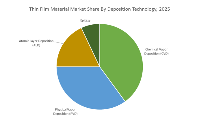
Market Share by Deposition Technology: Chemical Vapor Deposition Leads Through Superior Conformality, Material Versatility, and High-Throughput Manufacturing
Chemical Vapor Deposition (CVD) holds the dominant 40% share in the Thin Film Material Market because it is the only deposition technology that simultaneously delivers uniform conformality, broad material compatibility, and industrial-scale throughput, all of which are essential for modern semiconductor fabrication. As microchip architectures evolve toward increasingly intricate 3D geometries—deep trenches, high-aspect-ratio vias, stacked transistors, and multi-level interconnects—CVD remains indispensable due to its ability to grow films uniformly along every surface of a structure rather than coating only line-of-sight areas, as is typical with PVD processes. This superior step coverage is crucial for insulating and passivating advanced semiconductor features using dielectric materials such as SiO₂ and Si₃N₄, where even minor thickness variations can cause device failure. Additionally, CVD supports a wide material library, including polycrystalline silicon, metal films like tungsten, and numerous compound semiconductors—enabling manufacturers to deposit the precise compositions required for logic, memory, and power device architectures.
From a production standpoint, CVD offers a strategic balance between precision and throughput. While ALD excels in atomic-scale control, it is comparatively slow; CVD variants such as LPCVD and PECVD achieve significantly higher deposition rates, making them ideal for building thicker or non-critical layers at lower cost and higher efficiency. These attributes align with semiconductor manufacturers’ need for scalable, repeatable, and high-purity thin-film fabrication, securing CVD’s position as the most widely adopted and economically vital deposition technology across the thin film materials supply chain.
Market Share by Application: Semiconductors & ICs Dominate Through Extremely High Layer Requirements and Atomic-Level Precision Needs
Semiconductors & ICs account for the largest 45% share of the Thin Film Material Market, driven by the unparalleled complexity, layer density, and precision requirements embedded in today’s chip manufacturing processes. Advanced CPUs, GPUs, AI accelerators, and memory devices require 100 to 1,000+ individual thin-film layers—encompassing insulators, conductors, semiconductors, and barrier coatings—each deposited with extreme accuracy to ensure proper device functionality. This staggering layer count alone makes the semiconductor industry the most intensive consumer of deposition materials globally. Thin films form the dielectric insulation that separates transistor gates and interconnects, where dielectric strengths exceeding 10⁶ V/cm and ultra-low defect densities are essential to avoid electrical leakage, short circuits, and long-term reliability failures.
The segment’s leadership is further reinforced by the semiconductor industry’s relentless push toward miniaturization, especially as process nodes advance to 5 nm, 3 nm, and beyond. At these scales, the thickness of critical layers—such as gate oxides—shrinks to only a few atomic layers, requiring deposition technologies capable of delivering atomic-level uniformity, pinhole-free coverage, and tight material composition control. CVD, PECVD, and ALD are therefore foundational to enabling transistor scaling, power efficiency improvements, and the continued extension of Moore’s Law. As the world’s demand for computing, AI, cloud infrastructure, and high-performance devices accelerates, the semiconductor sector’s reliance on sophisticated thin-film materials ensures its position as the dominant application driving long-term market growth.
Country Analysis: Global Thin Film Material Development Hubs
Japan – Global Leadership in Ultra-High Purity PVD Targets, EUV Mask Blanks, and Advanced Oxide Semiconductor Materials
Japan continues to dominate the global Thin Film Material Market due to its unparalleled capability in ultra-high-purity metallization materials, EUV optical substrates, and oxide semiconductor targets, all of which are core enablers of next-generation semiconductors and displays. Japanese suppliers like JX Advanced Metals deliver 6N (99.9999%) purity copper sputtering targets—critical for Cu interconnect seed layers in sub-10 nm logic processes, where a single impurity can compromise electromigration reliability and long-term device performance. Japan’s vertically integrated ecosystem extends into Titanium (Ti) sputtering targets with 4N5 purity for barrier and hard mask layers, demonstrating its unmatched depth in critical metallization supply chains.
Japan also leads the global production of EUV mask blanks, primarily through AGC Inc., which manufactures multilayer-coated, low thermal expansion glass substrates essential for EUV lithography. These blanks require atomic-level uniformity in Mo/Si multilayers, making Japan the only producer capable of meeting full-scale EUV production requirements. Further strengthening its technological lead, KOBELCO has introduced proprietary oxide semiconductor targets (KOS-B03C) achieving 20–30 cm²/Vs electron mobility, outperforming IGZO and enabling higher-speed embedded memory and edge AI device development. Complementing these materials, ULVAC continues to innovate in thin-film deposition equipment, particularly customized PVD and ALD systems for 300 mm wafer processing, reinforcing Japan’s position at the forefront of semiconductor thin film technology.
United States – ALD/CVD Equipment Innovation and Advanced Logic Material Requirements Driving Sub-5 nm Thin Film Evolution
The United States remains the center of thin-film equipment innovation, particularly in Atomic Layer Deposition (ALD), Chemical Vapor Deposition (CVD), and advanced etching systems critical for sub-5 nm semiconductor logic nodes. U.S. companies Applied Materials and Lam Research are the global standard-bearers for ultra-thin, conformal high-k dielectrics, metal gates, barrier layers, and selective deposition films. Their ALD/CVD platforms enable atomic-scale thickness control, which is essential for FinFET, GAAFET, and backside power distribution architectures in advanced logic chips. The rise of AI accelerators is further accelerating demand for precisely engineered thin films with extremely low defectivity and optimized electrical properties.
In March 2024, Lam Research expanded into the pulsed laser deposition (PLD) segment to support complex thin films used in RF devices, power amplifiers, and MEMS microphones, where tight control over crystalline structure and stoichiometry is mandatory. Complementing this ecosystem, U.S.-based thin film equipment firms such as Denton Vacuum have broadened the adoption of Ion Beam Sputtering (IBS) systems, which deliver ultra-smooth, ultra-dense films for precision optics, EUV components, and high-frequency semiconductor devices. This positions the U.S. as a critical hub for the ALD/PLD/IBS infrastructure that underpins every major advancement in semiconductor scaling.
South Korea – OLED Encapsulation Materials and ALD-Driven 3D NAND Thin Film Engineering
South Korea’s leadership in OLED displays and memory semiconductors ensures the country remains at the forefront of thin film material usage and deposition process innovation. Samsung Display and LG Display have scaled the most advanced thin-film encapsulation (TFE) systems in the world, using ALD-based Al₂O₃ and multilayer organic/inorganic stacks to achieve the ultra-low oxygen and moisture transmission rates required for flexible, foldable, and rollable OLED panels. The need for ultra-thin, crack-resistant, optically clear barriers is driving continuous R&D in hybrid organo-inorganic thin film materials.
In memory, South Korean companies dominate 3D NAND production, which relies heavily on ALD to deposit precise SiO₂ and SiN films for the vertical channel structures of 176-layer and 200+ layer NAND. These extremely high-aspect-ratio structures cannot be realized without specialized ALD precursors and high-conformality deposition techniques. As Korean firms push into 3D DRAM and next-generation NAND architectures, material requirements are intensifying around stress-managed dielectrics, low-defect nitrides, and high-k interface layers, cementing South Korea’s global position in the Thin Film Material Market.
India – Thin Film Solar Cell Manufacturing Accelerated by PLI Incentives and ALMM Compliance
India is rapidly emerging as an important player in the Thin Film Material Market due to its strong push for domestic thin film solar PV manufacturing. Under the government’s Production Linked Incentive (PLI) scheme, fully integrated thin film module factories are explicitly recognized as compliant with domestic sourcing requirements—an incentive that has triggered new investment in thin-film deposition lines for CdTe, CIGS, and advanced TFPV architectures. As of April 2025, India has established 3.2 GW of fully integrated thin film solar module manufacturing capacity, operating independently of imported cells, wafers, or polysilicon.
Regulatory momentum continues with amendments to the Approved List of Models and Manufacturers (ALMM), effective June 2026, which certify thin film modules from integrated units as compliant with upcoming domestic cell sourcing mandates. These regulatory shifts are pushing India toward greater adoption of sputtering targets, absorbers, transparent conductive oxides (TCOs), buffer layers, and encapsulation films required for thin film photovoltaic manufacturing. Combined with strong energy security priorities, India is positioning itself as a fast-growing hub for thin film solar materials in the Asia-Pacific region.
Germany – Advanced PVD/CVD Equipment for Compound Semiconductors and High-Precision Thin Film Engineering
Germany remains a powerhouse in thin film deposition equipment for compound semiconductors, specialty optics, and high-power electronics. AIXTRON SE leads the global market for MOCVD systems, supporting epitaxial growth of GaN, SiC, and GaAs thin films used in LEDs, power electronics, RF amplifiers, and next-generation optoelectronic devices. Germany’s expertise in compound semiconductor manufacturing makes it a critical supplier for electric vehicle inverters, 5G base stations, and high-efficiency optical communication components.
Germany’s engineering strengths extend to precision PVD and etching systems through companies such as FHR Anlagenbau GmbH and scia Systems GmbH, which specialize in large-area coating, magnetron sputtering, ion beam etching, and customized thin film machinery. These systems are widely used in optical coatings, architectural glass, energy harvesting films, and industrial surface engineering, requiring extremely high uniformity, repeatability, and vacuum stability. Germany’s role as an equipment innovation hub positions it as a key enabler of both silicon and non-silicon thin film technology globally.
Competitive Landscape: Thin-Film Leaders Transforming Global Semiconductor Materials Supply
The competitive landscape is shaped by companies mastering ultra-high-purity manufacturing, precursor innovation, advanced target metallurgy, and deposition equipment integration. Their strategies reflect the industry's push toward sub-5 nm nodes, AI accelerators, advanced packaging, and sustainable material innovation.
Merck KGaA is a dominant force in ALD/CVD materials, supplying organometallic precursors for Mo, W, Zr, Ru, Y, and Nb, along with SODs and specialty gases. Its €500 million Kaohsiung megasite launched in December 2025 significantly enhances semiconductor material availability near Taiwan’s foundry ecosystem. The company is deeply embedded in materials innovation for GAA transistors, 3D NAND, and DRAM capacitor scaling, offering ppb-purity solutions required for sub-5 nm production. Merck’s integration of digital twin analytics into material optimization allows extremely stable batch-to-batch consistency, directly impacting high-volume manufacturing yields for customers.
DuPont’s electronics portfolio spans dry-film photoresists (Riston™), dielectric systems, metallization chemistries, and specialty thin-film materials. Its CYCLOTENE™ DF-PID launch in June 2025 positioned the company as a technological leader in void-free TGV filling for glass substrates, a cornerstone for advanced Fan-Out and chiplet packaging. DuPont’s Microfill™ plating chemistry supports uniform copper deposition for large AI substrates, improving signal integrity and reliability. Its sustainability milestone—a 58% reduction in emissions by February 2025—strengthens its appeal among semiconductor OEMs prioritizing ESG-compliant suppliers.
Umicore specializes in high-purity sputtering targets and evaporation materials used in PVD processes for semiconductors, optics, and displays. Its expertise includes producing multi-element alloy targets with composition accuracy within ±0.5 wt%, metallic purity up to 4N, and consistent fine-grain microstructures critical for uniform thin-film deposition. Proprietary flux-free solder bonding methods allow fabrication of ∅450 mm single-piece targets, supporting advanced packaging and next-generation memory device requirements. Umicore is expanding its portfolio into SiC, WTi, and Au/NiV targets to address emerging power electronics applications.
As a leading producer of high-purity PVD sputtering targets for logic, DRAM, and NAND, JX Nippon plays a central role in global thin-film metallization. The company’s November 2025 acquisition in Arizona expands its U.S. footprint, supporting domestic semiconductor initiatives and ensuring stable supply for newly built fabs. JX Nippon is investing aggressively in achieving 6N (99.9999%) purity for next-generation target materials, improving film reliability and reducing defect density. Its close collaboration with equipment OEMs ensures optimized target performance and sputtering efficiency across advanced PVD systems.
TEL is a global leader in ALD and CVD equipment, directly shaping material consumption patterns through its advanced deposition system architectures. The company’s innovations in PEALD, radical-driven deposition, and HVM ALD platforms are critical for the fabrication of 3D NAND, DRAM, and leading-edge logic. Its extensive installed base across Asia ensures that material suppliers aligned with TEL tools benefit from stable, long-term demand. TEL’s technology leadership allows the processing of increasingly complex metal oxide and nitride precursor families at lower thermal budgets, supporting the industry's progression toward sub-5 nm and beyond.
Thin Film Material Market
|
Parameter
|
Details
|
|
Market Size (2025)
|
$20.5 Billion
|
|
Market Size (2035)
|
$33.1 Billion
|
|
Market Growth Rate
|
4.9%
|
|
Segments
|
By Material Type (High-Purity Metals, Compounds, Semiconductor Materials, Precursor Gases), By Deposition Technology (Physical Vapor Deposition, Chemical Vapor Deposition, Atomic Layer Deposition, Epitaxy), By Application (Semiconductors & ICs, Energy, Displays & Optics, Sensors & MEMS, Wear & Corrosion Protection), By End-Use Industry (Electronics & IT, Energy, Aerospace & Defense, Automotive)
|
|
Study Period
|
2019- 2024 and 2025-2034
|
|
Units
|
Revenue (USD)
|
|
Qualitative Analysis
|
Porter’s Five Forces, SWOT Profile, Market Share, Scenario Forecasts, Market Ecosystem, Company Ranking, Market Dynamics, Industry Benchmarking
|
|
Companies
|
Resonac Corporation, JX Advanced Metals Corporation, Umicore N.V., AGC Inc., Materion Corporation, Applied Materials Inc., Lam Research Corporation, Tokyo Electron Limited, ASM International N.V., Solvay S.A., AIXTRON SE, Kobe Steel Ltd., Denton Vacuum Inc.
|
|
Countries
|
US, Canada, Mexico, Germany, France, Spain, Italy, UK, Russia, China, India, Japan, South Korea, Australia, South East Asia, Brazil, Argentina, Middle East, Africa
|
Thin Film Material Market Segmentation
By Material Type
- High-Purity Metals
- Compounds
- Semiconductor Materials
- Precursor Gases
By Deposition Technology
- Physical Vapor Deposition (PVD)
- Chemical Vapor Deposition (CVD)
- Atomic Layer Deposition (ALD)
- Epitaxy
By Application
- Semiconductors & ICs
- Energy
- Displays & Optics
- Sensors & MEMS
- Wear & Corrosion Protection
By End-Use Industry
- Electronics & IT
- Energy
- Aerospace & Defense
- Automotive
By Region
- North America (United States, Canada, Mexico)
- Europe (Germany, France, United Kingdom, Spain, Italy, Rest of Europe)
- Asia Pacific (China, India, Japan, South Korea, Australia, Rest of APAC)
- South and Central America (Brazil, Argentina, Rest of SCA)
- Middle East and Africa (Saudi Arabia, UAE, South Africa, Rest of Middle East, Rest of Africa)
Top Companies: Key Thin Film Material Manufacturers
- Resonac Corporation (Showa Denko/Hitachi Chemical)
- JX Advanced Metals Corporation
- Umicore N.V.
- AGC Inc.
- Materion Corporation
- Applied Materials Inc.
- Lam Research Corporation
- Tokyo Electron Limited (TEL)
- ASM International N.V.
- Solvay S.A.
- AIXTRON SE
- KOBE STEEL, LTD. (KOBELCO)
- Denton Vacuum, Inc.
