
Larger AI packages, rapidly scaling HBM, shrinking interconnect pitches and kilowatt-class accelerators are raising requirements for substrates, molding compounds, underfills, thermal interfaces, dielectrics, plating chemistries and CMP materials.
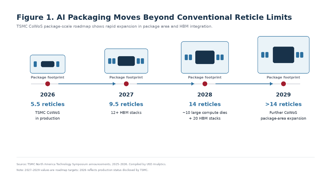
AI accelerator development is shifting more system performance into the package. Rather than relying only on transistor scaling, semiconductor manufacturers are integrating more compute dies, larger HBM configurations and increasingly dense die-to-die connections within heterogeneous architectures. TSMC is already producing 5.5-reticle-size CoWoS and plans a 14-reticle version capable of integrating approximately 10 large compute dies and 20 HBM stacks in 2028. Intel separately says its packaging capability can scale to eight times the conventional reticle limit today and more than 12 times by 2028.
The materials implication is substantial. More package area increases sensitivity to warpage and dimensional stability; taller and denser HBM stacks intensify underfill and molding requirements; finer Cu interconnects demand tighter CMP and surface preparation; and accelerator board power has already reached 1,400 W in commercially specified platforms. These pressures are creating new value pools across semiconductor packaging materials while making qualification, co-development and process integration increasingly important barriers to entry.
Executive Takeaways
- AI packaging is moving far beyond conventional package dimensions. TSMC's roadmap progresses from 5.5-reticle CoWoS in production to 9.5 reticles in 2027 and 14 reticles in 2028, with increasingly large HBM configurations.
- HBM packaging chemistry is becoming a competitive technology layer. SK hynix is scaling Advanced MR-MUF while Samsung continues advancing TC-NCF, demonstrating that thinner dies, tighter gaps, heat transfer and warpage are being solved through competing materials architectures.
- Hybrid bonding is pulling semiconductor process chemistry deeper into advanced packaging. Imec has demonstrated 2 µm die-to-wafer hybrid bonding and 200 nm wafer-to-wafer bonding, with stringent requirements for Cu planarity, surface cleanliness and overlay.
- Thermal management is moving into the critical path. AI accelerators are reaching 1,000–1,400 W board power, while packaging-material suppliers are developing micron-scale fillers, lower-impedance TIMs and more thermally efficient encapsulation systems.
Key Metrics Reshaping AI Semiconductor Packaging
Table 1. Key Metrics Reshaping AI Semiconductor Packaging
|
Indicator |
Current benchmark |
Strategic Significance |
|
Current TSMC CoWoS scale |
5.5 reticles |
Demonstrates package-area expansion already in production |
|
TSMC 2028 CoWoS roadmap |
14 reticles |
Indicates further scaling of heterogeneous integration |
|
HBM integration at 14 reticles |
~20 HBM stacks |
Increases thermal, substrate and interconnect complexity |
|
HBM4 interface |
2,048 I/Os |
Doubles interface width versus previous-generation HBM |
|
W2W hybrid-bonding demonstration |
200 nm pitch |
Pushes bonding toward nanoscale interconnect density |
|
W2W post-bond overlay |
<40 nm |
Illustrates required manufacturing precision |
|
TIM filler / package gap example |
~1 µm / 7 µm |
Shows formulation pressure created by shrinking gaps |
|
2026 assembly & packaging equipment sales |
$6.7B |
Evidence of expanding investment in semiconductor back-end infrastructure |
Sources: TSMC, SK hynix, imec/EV Group, SEMI and Henkel.
AI Compute Shifts Scaling from the Die to the Package
The AI compute roadmap is creating packages that behave increasingly like integrated systems rather than conventional chip carriers. TSMC plans to move 9.5-reticle-size CoWoS into volume production in 2027 with 12 or more HBM stacks, followed by its approximately 14-reticle architecture in 2028. The latter is designed to integrate roughly 10 large compute dies and 20 HBM stacks. TSMC subsequently expects CoWoS configurations larger than 14 reticles in 2029.
Intel provides a second signal that this is an architectural shift rather than a single-foundry roadmap. Its New Mexico advanced-packaging operations describe packages reaching eight times the conventional reticle limit today and more than 12 times by 2028, using Foveros stacking, embedded silicon bridges and newer EMIB-T architectures. As package dimensions increase, substrate flatness, CTE control, underfill flow, molding stress, power delivery and thermal expansion become design constraints that cannot be solved by silicon scaling alone.
TSMC plans a 14-reticle CoWoS architecture for 2028 capable of integrating approximately 10 large compute dies and 20 HBM stacks—illustrating how AI scaling is moving increasingly into the package.
HBM Bandwidth and Stack Density Push Packaging Materials Into the Critical Path
High-bandwidth memory is reinforcing the move toward materials-intensive heterogeneous integration. Micron's 12-high HBM3E benchmark exceeds 1.2 TB/s per stack, while its 36 GB 12-high HBM4 entered high-volume production in 2026 at more than 2.8 TB/s and greater than 11 Gb/s pin speed. Samsung's 12-layer HBM4E samples reach up to 3.6 TB/s per stack, with pin speed scalable to 16 Gb/s.
Interface width is also increasing. SK hynix's HBM4 uses 2,048 I/O channels—twice the previous generation—and the company reports more than a 40% improvement in power efficiency. These changes place simultaneous pressure on interconnect density, power delivery, die thickness, thermal paths and mechanical integrity. Higher bandwidth therefore creates demand not only for faster DRAM but for more capable molding compounds, underfills, bonding technologies, thermal interfaces and package substrates.
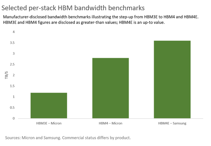
Micron's HBM4 figure represents high-volume production, while Samsung's HBM4E figure represents customer samples rather than mass production. The chart should therefore be read as a technical bandwidth progression, not as a like-for-like commercial market comparison.
HBM Packaging Chemistry Becomes a Competitive Technology Platform
HBM scaling exposes a less visible but commercially important materials contest: how to connect, insulate and mechanically stabilize increasingly thin DRAM dies. SK hynix moved from TC-NCF to Mass Reflow Molded Underfill in HBM2E and subsequently developed Advanced MR-MUF for higher-layer products. Its 12-layer HBM3 maintained the same overall thickness while using DRAM chips that were 40% thinner and separated by a 13% narrower gap than the preceding architecture. SK hynix used a new epoxy molding compound and a vacuum/pressure filling process to manage warpage, fill tighter spaces and improve heat transfer.
The material architecture is significant because MR-MUF combines mass reflow with a liquid epoxy molding compound that fills spaces between stacked dies and bumps. SK hynix says the original MR-MUF improved HBM2E heat dissipation by 36% compared with HBM2, while the EMC developed for Advanced MR-MUF offered 1.6 times the heat-dissipation properties of its earlier EMC. Its 12-layer HBM3 development also produced approximately threefold productivity and around 2.5 times heat-dissipation improvement in the company's process comparison. These figures are SK hynix-specific development results, not universal MR-MUF performance benchmarks.
Samsung has taken a different route. Its 12-high HBM3E uses Advanced TC-NCF, with film thickness reduced sufficiently to create a 7 µm inter-chip gap while maintaining the same overall package-height specification as its eight-layer architecture. Samsung also varies bump dimensions, using smaller bumps for signaling and larger bumps where additional heat dissipation is required. The competing approaches demonstrate that HBM packaging is not converging on one material system; instead, suppliers are co-optimizing adhesive films, liquid molding compounds, bump structures and process conditions around stack density, yield and thermal performance.
Higher-layer HBM is forcing material redesign at micron-scale geometries: SK hynix has used 40% thinner DRAM dies, while Samsung has demonstrated inter-chip gaps as small as 7 µm.
Hybrid Bonding Compresses Interconnect Pitch and Raises Process-Chemistry Precision
The move from solder-based interconnects toward direct copper hybrid bonding changes the chemistry and surface-control requirements of advanced packaging. Imec demonstrated die-to-wafer Cu/SiCN hybrid bonding at 2 µm Cu pad pitch, with less than 350 nm placement overlay error, Kelvin electrical yield above 85% and daisy-chain yield above 70% on its research vehicle. Achieving that pitch required Cu pad recess below 2.5 nm, making CMP control, particle removal, surface cleanliness and singulation quality integral to bonding performance.
The roadmap is already moving substantially below the die-to-wafer scale. In May 2026, imec and EV Group demonstrated wafer-to-wafer hybrid bonding at 200 nm interconnect pitch and achieved a Cu pad-to-pad post-bond overlay vector below 40 nm across 100% of dies on a full 300 mm wafer. Imec had previously demonstrated 400 nm wafer-to-wafer pitch and characterizes solder-based die-to-wafer bonding as likely to encounter a practical scaling limit in roughly the 10–5 µm range.
At 200 nm interconnect pitch, imec and EV Group achieved post-bond Cu pad overlay below 40 nm across every die on a 300 mm research wafer.
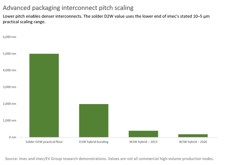
The key materials implication is not simply smaller copper pads. Moving from micron-scale solder connections toward sub-micron Cu/SiCN bonding raises the value of CMP slurries, post-CMP cleaning chemistries, dielectric materials, wafer-surface preparation and contamination control because increasingly small topography or particle defects can compromise the bonding interface.
Glass Substrates Target the Warpage and Routing-Density Limits of Organic Packaging
As heterogeneous packages expand in area, substrate dimensional stability becomes more important. Intel argues that glass can tolerate higher process temperatures, reduce pattern distortion by 50%, and potentially enable a 10-fold increase in interconnect density compared with today's organic substrate approach. The company is targeting glass first at large-form-factor AI, data-center and graphics applications and in July 2026 announced a collaboration with Lens Technology focused on scaling glass-substrate packaging.
The emerging supply ecosystem is also beginning to expose manufacturability metrics. AGC advertises glass compositions from approximately 0.1 mm to 1.1 mm and above, TGV capability at pitches of 50 µm or greater, aspect ratios up to 20:1 at 1.0 mm thickness, and panel-format production such as 510 × 515 mm. It also positions adjustable CTE and higher modulus as tools for stress and warpage control. These are supplier-specific capabilities rather than universal glass-substrate specifications, but they show that commercialization depends on via processing, panel handling, metallization and yield—not merely favorable bulk glass properties.
Glass remains an emerging architecture alongside organic substrates, silicon interposers and embedded bridges, not as an immediate universal replacement. The commercial opportunity lies in applications where larger package footprints, tighter layer-to-layer registration, lower warpage and dense routing justify the additional process development and qualification burden.
Kilowatt-Class AI Accelerators Push Thermal Interfaces Into the Critical Path
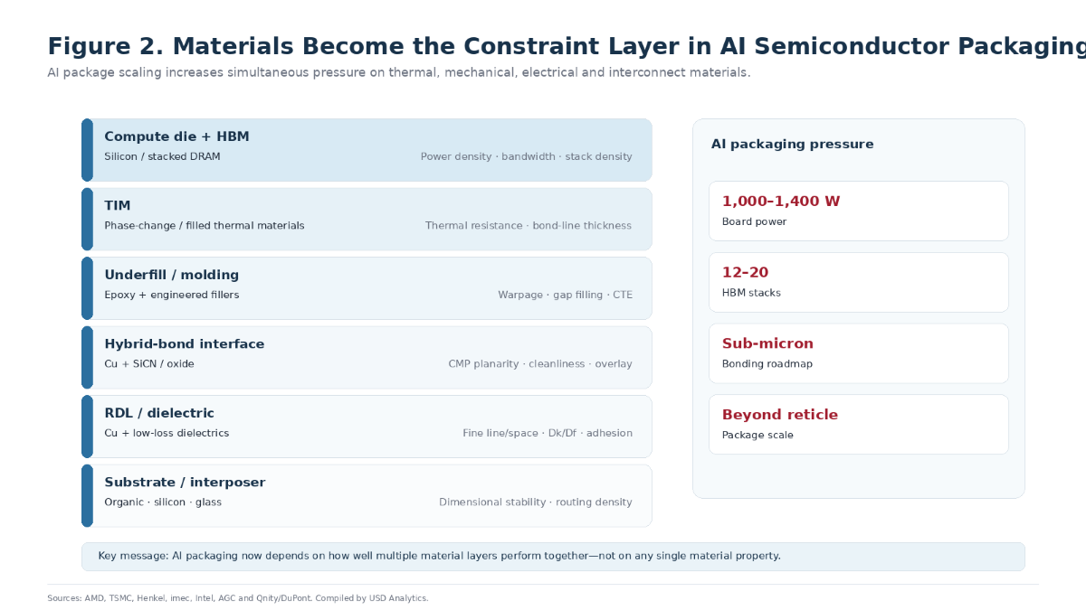
Thermal management is becoming inseparable from package architecture. AMD's MI350X is specified at 1,000 W typical board power, while the direct-liquid-cooled MI355X reaches 1,400 W. The MI355X combines 288 GB HBM3E with 8 TB/s of memory bandwidth, illustrating how compute power, memory bandwidth and package thermal loading are rising together.
At the material interface, bulk thermal conductivity alone is not sufficient. Bond-line thickness, contact resistance, pressure, mechanical stress, pump-out behavior and long-term reliability can determine effective package performance. Henkel's commercial Bergquist Hi Flow THF 5000UT phase-change TIM, for example, reports thermal conductivity up to 8.5 W/m·K, thermal impedance of 0.04°C·cm²/W at 35 psi and 0.06°C·cm²/W below 10 psi, with reliability evaluation up to 150°C. These are product-specific values, but they illustrate the performance dimensions suppliers must simultaneously optimize.
Geometry adds another constraint. At SEMICON Europa 2025, Henkel reported developing approximately 1 µm filler particles capable of filling package gaps as small as 7 µm. The implication is that next-generation thermal and encapsulation materials increasingly require controlled particle-size distribution and rheology in addition to higher thermal conductivity.
Figure 2. Materials Become the Constraint Layer in AI Semiconductor Packaging
Fine RDL, Dielectrics, CMP and Plating Chemistry Gain Strategic Value
Advanced packaging is also increasing process intensity at the redistribution and bonding layers. Qnity/DuPont states that Cu RDL requirements have tightened from approximately 5 µm line/space toward 2 µm line/space, with high-purity electroplating chemistry required to maintain fine-feature uniformity and via filling. Its packaging-dielectric portfolio emphasizes low cure temperature, low electrical loss, thermal stability, chemical resistance and high resolution across BCB- and epoxy-based platforms.
Hybrid bonding amplifies this chemistry requirement. Imec's need to keep Cu pad recess below 2.5 nm before 2 µm-pitch bonding demonstrates how CMP shifts from conventional planarization toward a direct determinant of bonding yield. Post-CMP cleaning must preserve smooth Cu and dielectric surfaces while controlling particles and corrosion, and increasingly dense package routing places greater emphasis on deposition uniformity, photoresist resolution, dielectric cure conditions and copper topography.
Table 2. Advanced Packaging Materials and Performance Requirements
|
Material system |
Primary package role |
Critical performance requirements |
Emerging pressure |
|---|---|---|---|
|
Organic / glass / silicon substrates |
Mechanical platform and signal routing |
Dimensional stability, CTE, flatness, routing density |
Larger package area and chiplet count |
|
HBM underfill / molding compounds |
Gap filling, protection and stress management |
Rheology, filler control, CTE, thermal transport, void control |
Thinner dies and tighter stack gaps |
|
Thermal interface materials |
Die-to-lid / lid-to-cooling heat transfer |
Low thermal impedance, thin bond line, reliability |
Kilowatt-class accelerator power |
|
Packaging dielectrics |
RDL insulation and passivation |
Low loss, resolution, low cure temperature, adhesion |
Higher-frequency and finer routing |
|
Cu plating / CMP / cleaning |
RDL and hybrid-bond interfaces |
Uniformity, purity, planarity, defect control |
2 µm to sub-micron interconnect scaling |
|
Electronic adhesives / lid attach |
Structural attachment |
Low stress, adhesion, thermal cycling reliability |
Larger, thinner and more heterogeneous packages |
Sources: Intel, AGC, SK hynix, Samsung, Henkel, imec and Qnity/DuPont.
Warpage, Reliability and Yield Become Multi-Material Problems
Larger package areas amplify CTE mismatch and warpage, while thinner dies and smaller interconnects increase sensitivity to local stress and contamination. SEMI's advanced-packaging discussions identify electromigration, corrosion and thermomechanical degradation as increasingly interconnected failure mechanisms rather than isolated reliability events.
Hybrid bonding is also making yield economics more architecture-dependent. Imec's 2 µm die-to-wafer test vehicle achieved above 85% Kelvin electrical yield and above 70% daisy-chain electrical yield, while the institute notes that die-to-wafer bonding can improve compound-yield economics because known-good dies can be selected before stacking. These are R&D results, not commercial manufacturing yields, but they demonstrate why surface defects, die placement accuracy and process variation become economically more consequential as package value rises.
For materials suppliers, this favors technologies that improve process windows, not merely datasheet maxima. A slightly lower-conductivity material that delivers better dispense consistency, lower stress or higher bonding yield can be commercially preferable to a laboratory material with superior bulk properties but narrow manufacturing tolerances.
High-Purity Fillers and Specialty Raw Materials Move Up the Strategic Agenda
The AI packaging opportunity extends upstream from formulated underfills and TIMs into engineered filler and resin systems. Advanced MR-MUF uses epoxy molding compounds to fill increasingly narrow HBM gaps, while AGC is developing both hollow and solid silica fillers for low-Dk and low-Df electronic applications. Henkel's move toward approximately 1 µm fillers shows how particle morphology and size distribution increasingly determine whether a formulation can physically enter next-generation package geometries.
This creates an opportunity for suppliers of spherical silica, high-purity resins, coupling agents, low-loss polymers, specialty curing systems and semiconductor-grade fillers. Qualification barriers are likely to remain substantial because changes in filler loading or resin chemistry can alter viscosity, CTE, modulus, moisture behavior, dielectric performance, package stress and reliability simultaneously. For high-value AI packages, the commercial advantage may therefore sit with suppliers capable of application-specific co-formulation and long-duration qualification, rather than commodity raw-material supply alone.
AI Investment Is Pulling Capital Toward Packaging and Test Infrastructure
Capital spending is moving toward the semiconductor back end as advanced packaging becomes necessary for AI and HBM. SEMI reports that assembly and packaging equipment sales increased 20.8% in 2025 and are projected to grow another 9.6% to $6.7 billion in 2026, reaching $8.6 billion in 2028. Test equipment sales are projected to reach $15.3 billion in 2026 after a 55.3% increase in 2025, reflecting the rising complexity and reliability burden of AI devices.
The materials market is moving in the same direction. SEMI reported that semiconductor packaging-material revenue increased 9.3% to $27.4 billion in 2025, with advanced substrates among the contributors to growth. That does not isolate AI packaging materials, but it confirms that materials demand is expanding alongside equipment and process complexity.
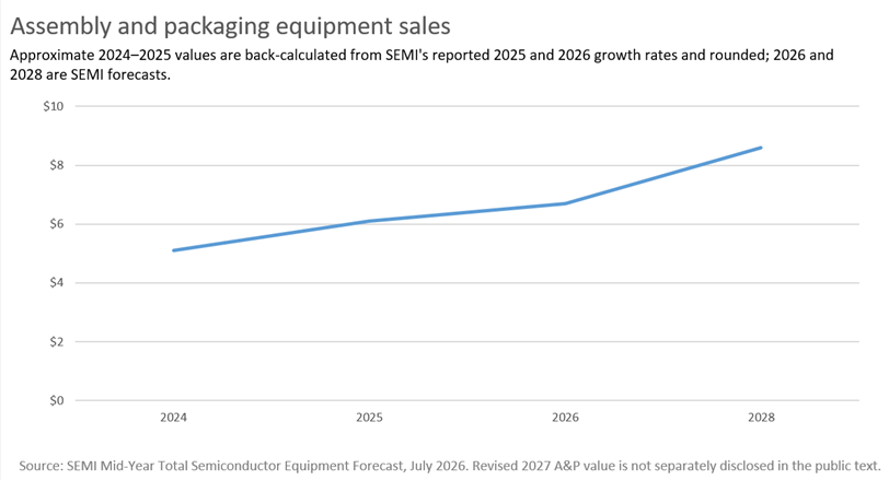
The approximately $5.1 billion 2024 and $6.1 billion 2025 values are calculated from SEMI's reported 20.8% growth in 2025 and 9.6% growth to $6.7 billion in 2026, so they should remain visually marked as approximate. The 2026 and 2028 values are directly disclosed forecasts.
Manufacturer Investments Show Advanced Packaging Becoming Strategic Infrastructure
Corporate spending is reinforcing the technical evidence. SK hynix is investing approximately $3.87 billion in an Indiana advanced-packaging and R&D facility focused on next-generation HBM, with mass production targeted for the second half of 2028. Intel's Fab 9 in New Mexico forms part of a $3.5 billion investment in high-volume advanced semiconductor packaging, including Foveros.
TSMC's expanded U.S. investment plan now totals $165 billion and includes two planned advanced-packaging facilities alongside additional fabs and R&D infrastructure. The full $165 billion should not be treated as packaging investment, but the inclusion of dedicated packaging facilities demonstrates that leading-edge manufacturing localization is expanding beyond wafer fabrication.
Table 3. Manufacturer Investment and Technology Signals in AI Advanced Packaging
|
Company |
activity |
Commercial signal |
|---|---|---|
|
TSMC |
5.5-reticle CoWoS in production; 14-reticle architecture planned for 2028 |
Package scaling is becoming central to AI compute roadmaps |
|
Intel |
$3.5B New Mexico advanced-packaging investment; glass collaboration with Lens Technology |
Packaging and alternative substrates moving toward manufacturing ecosystems |
|
SK hynix |
$3.87B Indiana HBM advanced-packaging/R&D investment |
HBM packaging capacity being localized closer to AI customers |
|
Samsung |
Commercial HBM4 plus HBM4E customer samples; Advanced TC-NCF development |
Memory, package design and thermal architecture increasingly co-developed |
|
Micron |
36 GB 12-high HBM4 in high-volume production at >2.8 TB/s |
Advanced stack packaging becoming a production differentiator |
|
Henkel |
1 µm-level filler development for ~7 µm package gaps |
Materials suppliers adapting formulations to shrinking geometries |
Sources: TSMC, Intel, SK hynix, Samsung, Micron and SEMI/Henkel.
Commercial Opportunity Moves From Material Supply Toward Application Engineering
The commercial opportunity in AI packaging varies across material classes. Glass substrates face long qualification and process-integration cycles; hybrid-bond chemistries must perform within nanometer-scale surface tolerances; HBM molding systems have to balance rheology, CTE, modulus and heat transport; and TIMs must achieve low effective thermal resistance without imposing damaging mechanical stress. The winning proposition is therefore increasingly material + process + qualification support, rather than chemistry supplied independently of the package architecture.
This favors suppliers able to work directly with foundries, memory manufacturers, OSATs and equipment companies during process development. It also raises entry barriers. A material can perform well in isolation yet fail because it changes warpage, cure behavior, copper topography, surface contamination, bonding alignment or long-term thermal cycling. Customer qualification and equipment compatibility can therefore become as important to competitive positioning as raw material performance.
Commercial value pools appear particularly attractive around HBM encapsulation and underfill systems, advanced thermal interfaces, glass-core and low-loss substrates, fine-line RDL materials, packaging dielectrics, Cu plating chemistry, CMP materials, post-CMP cleaning and electronic adhesives. These markets sit directly at the interfaces where AI packaging architectures are creating new physical constraints.
Strategic Outlook: Materials Will Determine How Far AI Packaging Can Scale
AI semiconductor packaging is entering a phase in which package architecture and material performance are increasingly inseparable. TSMC's progression toward 14-reticle CoWoS, HBM4's 2,048-channel interface, 200 nm research-scale hybrid bonding and 1,400 W accelerator board power demonstrate that several packaging variables are scaling simultaneously. The next bottleneck may therefore arise not from one material property but from the interaction between thermal transport, warpage, interconnect precision, electrical loss and manufacturing yield.
This favors a segmented materials transition rather than a single breakthrough technology. Organic substrates will continue to serve important architectures while glass develops in large-form-factor, density-sensitive applications. MR-MUF and TC-NCF will continue evolving while hybrid bonding moves deeper into production roadmaps. Polymer TIMs, phase-change materials and other thermal architectures will be selected according to package geometry and cooling design rather than conductivity alone.
The strategic opportunity for advanced-material suppliers is consequently broader than supplying higher-performance chemistry. AI packaging is creating demand for materials engineered around entire process windows—geometry, equipment, thermal behavior, electrical performance, reliability and yield. Suppliers that gain early qualification within HBM, glass-substrate, hybrid-bonding and high-density RDL ecosystems can become embedded in technology platforms whose switching costs are substantially higher than conventional materials procurement.
Related Advanced Semiconductor Packaging Research
For the related-research block, I would use these six reports from the USD Analytics catalogue:
Semiconductor and IC Packaging Materials Market
Polymer based Thermal Interface Materials Market
Low Dielectric Materials Market
Assess AI Packaging Materials, Technology Roadmaps and Supplier Opportunities
Access customized intelligence covering advanced semiconductor packaging materials, HBM integration, glass substrates, thermal interfaces, underfills, encapsulants, electronic adhesives, packaging dielectrics, CMP chemistry, fine-line metallization, supplier positioning and emerging qualification requirements across the AI semiconductor value chain.
Discuss Your Research Requirement
Key Government, Technical and Industry Authorities
U.S. Department of Commerce / CHIPS for America — semiconductor manufacturing incentives, advanced-packaging localization, supply-chain investment and U.S. semiconductor industrial strategy.
National Institute of Standards and Technology (NIST) — advanced semiconductor packaging R&D, metrology, materials, manufacturing technology and the National Advanced Packaging Manufacturing Program.
European Commission / European Chips Act — semiconductor capacity, advanced manufacturing, research infrastructure and European supply-chain resilience.
TSMC — CoWoS scaling, advanced 3D integration and AI package roadmaps.
Intel — Foveros, EMIB, U.S. advanced-packaging manufacturing and glass-substrate development.
SEMI — semiconductor equipment, packaging-material investment and advanced-packaging industry evidence.
imec — independent hybrid-bonding, CMP, overlay and interconnect-pitch research.
SK hynix — HBM packaging, MR-MUF, high-layer-count HBM and packaging investment.
Samsung Electronics — HBM4/HBM4E, TC-NCF and high-stack memory packaging.
Micron Technology — HBM3E/HBM4 bandwidth, stack scaling and high-volume production benchmarks.
Henkel — thermal interface materials, packaging fillers, underfills and semiconductor package-material integration.
AGC — glass-core substrates, through-glass vias, low-loss materials and semiconductor-grade fillers.
Qnity / DuPont Electronics — advanced RDL plating, packaging dielectrics, CMP and semiconductor process materials.